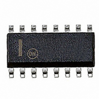
NE570DR2G ON Semiconductor, NE570DR2G Datasheet - Page 6

NE570DR2G
Manufacturer Part Number
NE570DR2G
Description
IC COMPANDOR DUAL GAIN 16-SOIC
Manufacturer
ON Semiconductor
Type
Compandorr
Datasheet
1.NE570DR2G.pdf
(10 pages)
Specifications of NE570DR2G
Applications
Cellular Radio, Players
Mounting Type
Surface Mount
Package / Case
16-SOIC (0.300", 7.5mm Width)
Operating Supply Voltage (typ)
9/12/15/18V
Operating Supply Voltage (min)
6V
Operating Supply Voltage (max)
24V
Operating Temp Range
0C to 70C
Operating Temperature Classification
Commercial
Package Type
SOIC W
Mounting
Surface Mount
Pin Count
16
Lead Free Status / RoHS Status
Lead free / RoHS Compliant
Other names
NE570DR2G
NE570DR2GOSTR
NE570DR2GOSTR
Available stocks
Company
Part Number
Manufacturer
Quantity
Price
Part Number:
NE570DR2G
Manufacturer:
ON/安森美
Quantity:
20 000
CIRCUIT DETAILS−RECTIFIER
averaging rectifier. The input current to the summing node
of the op amp, V
amp. If we can mirror the op amp output current into a
unipolar current, we will have an ideal rectifier. The output
current is averaged by R
constant, and then mirrored with a gain of 2 to become I
the gain control current.
amp is a one−stage op amp, biased so that only one output
device is on at a time. The non−inverting input, (the base of
Q
1.8 V V
(the emitters of Q
R1. The single diode between the bases of Q
that only one device is on at a time. To detect the output
current of the op amp, we simply use the collector currents of
the output devices Q
input swings positive and Q
swings negative. The collector currents will be in error by the
1
Figure 8 shows the concept behind the full−wave
Figure 9 shows the rectifier circuit in more detail. The op
), which is shown grounded, is actually tied to the internal
of Q
V
IN
REF
5
or Q
R
. The inverting input is tied to the op amp output,
1
Figure 8. Rectifier Concept
6
IN
5
on negative or positive signal swings,
−
+
and Q
I = V
/R
5
1
, is supplied by the output of the op
IN
and Q
5
/R
6
, C
C
), and the input summing resistor
1
R
R
, which set the averaging time
6
10 kW
5
. Q
conducts when the input
R
6
5
V+
will conduct when the
I
+1
−1
G
0
5
and Q
Figure 10. Rectifier Accuracy
6
RECTIFIER INPUT dBm
−40
assures
http://onsemi.com
G
,
NE570
−20
6
respectively. ICs such as this have typical NPN ’s of 200
and PNP ’s of 40. The ’s of 0.995 and 0.975 will produce
errors of 0.5% on negative swings and 2.5% on positive
swings. The 1.5% average of these errors yields a mere
0.13 dB gain error.
(typically 50 nA), will become significant as it must be
supplied by Q
coupling into the rectifier. If an offset voltage exists between
the V
V
cause an input current of 100 nA, which will produce twice
the error of the input bias current. For highest accuracy, the
rectifier should be coupled capacitively. At high input levels
the of the PNP Q
increasing error until the circuit saturates. Saturation can be
avoided by limiting the current into the rectifier input to
250 mA. If necessary, an external resistor may be placed in
series with R
shows the rectifier accuracy versus input level at a frequency
of 1.0 kHz.
OS
NOTE:
I
At very low input signal levels the bias current of Q
G
= 2
/R
IN
0
1
Figure 9. Simplified Rectifier Schematic
V
input pin and the base of Q
will be generated. A mere 1.0 mV of offset will
IN
R
Q
avg
1
1
1
Q
5
Q
. Another low level error can be caused by DC
2
I
to limit the current to this value. Figure 10
3
1
6
will begin to suffer, and there will be an
Q
4
V+
V−
D
I
2
1
Q
6
Q
5
Q
7
2
C
R
10 kW
R
10 kW
, an error current of
R
1
5
Q
8
V
IN
Q
9
2
,


