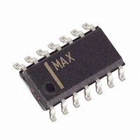
MAX4298ESD+ Maxim Integrated Products, MAX4298ESD+ Datasheet - Page 2

MAX4298ESD+
Manufacturer Part Number
MAX4298ESD+
Description
IC STEREO DVR AUDIO 14-SOIC
Manufacturer
Maxim Integrated Products
Type
PSRR Stereo Driverr
Datasheet
1.MAX4298ESDT.pdf
(14 pages)
Specifications of MAX4298ESD+
Applications
Desktop Audio, MP3, USB
Mounting Type
Surface Mount
Package / Case
14-SOIC (3.9mm Width), 14-SOL
Lead Free Status / RoHS Status
Lead free / RoHS Compliant
Supply Voltage (V
Standby Supply Voltage (SV
REG, FB, REGON to GND ..........................-0.3V to (V
BIAS, C
OUT_, MICOUT to GND ................................-0.3V to the Smaller
Duration of Output Short-Circuit to GND or V
ABSOLUTE MAXIMUM RATINGS
Ultra-High PSRR Stereo Drivers +
Microphone Amp + 100mA Linear Regulator
Stresses beyond those listed under “Absolute Maximum Ratings” may cause permanent damage to the device. These are stress ratings only, and functional
operation of the device at these or any other conditions beyond those indicated in the operational sections of the specifications is not implied. Exposure to
absolute maximum rating conditions for extended periods may affect device reliability.
ELECTRICAL CHARACTERISTICS
(V
wise noted. Load resistors (R
MAX4299, unless otherwise noted.) (Note 1)
2
Supply Voltage Range
Quiescent Current
Mute Quiescent Current
SV
DRIVER AMPLIFIERS
Input Offset Voltage
Input Bias Current
Power-Supply Rejection
Ratio
Output Drive
THD + Noise
Full-Scale Signal-to-Noise Ratio
(Note 4)
Capacitive Drive
Open-Loop Voltage Gain
Unity-Gain Bandwidth
CC
CC
_______________________________________________________________________________________
= SV
BYPASS
Current (Note 2)
CC
PARAMETER
= +5V, R
, MUTE, IN_, MICIN to GND ..............-0.3V to the
CC
) to GND ...............................................+6V
L
=
Larger of (V
CC
on all outputs, C
L
) are terminated to 2.25V. Typical values are at T
) to GND ...............................+6V
CC
SYMBOL
of +5.5V, or (V
I
PSRR
V
A
GBW
I
SVCC
SNR
V
V
+0.3V) or (SV
BIAS
I
OUT
VOL
CC
CC
OS
CC
BYPASS
................10min
Inferred from PSRR test
MAX4298
MAX4299
MAX4298
MAX4299
V
V
DC, V
f = 20kHz
f = 100kHz
R
R
R
A
V
A
V
A
V
R
V
R
BIAS
BIAS
OUT
OUT
OUT
OUT
L
L
L
V
V
V
L
L
= 10k
= 32
= 16
= 10k ,
= 32 , 0.55V
CC
= -1V/V, f = 1kHz, R
= -1V/V, f = 1kHz, R
= -1V/V, f = 1kHz, R
CC
CC
= 1µF, C
= 1.5V
= 1.2V
= 1.0V
= 1.06V
CC
+ 0.3V)
= 1.125V, V
= 2.25V, V
+ 0.3V)
+0.3V)
= 4.5V to 5.5V
RMS
RMS
RMS
BIAS
RMS
CONDITIONS
, (Notes 3, 4)
CC
, A
= 1µF, C
CC
V
OUT
Continuous Power Dissipation
Operating Temperature Range ..........................-40 C to +85 C
Storage Temperature Range .............................-65 C to +150 C
Lead Temperature (soldering, 10s) .................................+300 C
= 5.0V
V
= 0
= -1V/V
10-Pin µMAX (derate 5.6mW/ C above +70 C) ...........444mW
14-Pin SO (derate 8.3mW/ C above +70 C)................667mW
20-Pin SO (derate 10.0mW/ C above +70 C)..............800mW
16-Pin TSSOP (derate 9.4mW/ C above +70 C) .........755mW
L
L
L
= 32 ,
= 16 ,
= 10k ,
V
REG
CC
A
= 10µF (MAX4299), T
- 0.55V
= +25°C. Specifications apply to both MAX4298 and
MIN
1.45
4.5
1.2
1.0
76
A
= T
0.0008
MIN
TYP
10.2
10.6
10.2
10.6
1.59
1.53
1.48
0.02
0.04
300
115
105
0.2
1.3
93
80
22
87
7
1
to T
MAX
MAX
17.5
18.0
17.5
18.0
500
5.5
0.1
10
, unless other-
UNITS
V
MHz
mA
mA
mV
dB
dB
dB
nA
RMS
nF
%
V
A


