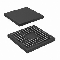
CLC5903SM/NOPB National Semiconductor, CLC5903SM/NOPB Datasheet - Page 21

CLC5903SM/NOPB
Manufacturer Part Number
CLC5903SM/NOPB
Description
IC DGTL TUNER/AGC DUAL 128-FBGA
Manufacturer
National Semiconductor
Type
Tunerr
Datasheet
1.CLC5903SMNOPB.pdf
(29 pages)
Specifications of CLC5903SM/NOPB
Applications
Base Stations
Mounting Type
Surface Mount
Package / Case
128-FBGA
Lead Free Status / RoHS Status
Lead free / RoHS Compliant
Other names
*CLC5903SM
*CLC5903SM/NOPB
CLC5903SM
*CLC5903SM/NOPB
CLC5903SM
Available stocks
Company
Part Number
Manufacturer
Quantity
Price
Company:
Part Number:
CLC5903SM/NOPB
Manufacturer:
Texas Instruments
Quantity:
10 000
SCK will be set to the proper strobe rate for each debug tap
point. POUT_EN and PSEL[2..0] have no effect in Debug
Mode. The outputs are turned on when the Debug Mode bit
is set. Normal serial outputs are also disabled.
Control Registers
The chip is configured and controlled through the use of 8-bit
control registers. These registers are accessed for reading or
Control Register Addresses and Defaults
DEC
DEC_BY_4
SCALE
GAIN_A
GAIN_B
RATE
SOUT_EN
SCK_POL
SFS_POL
RDY_POL
MUX_MODE
PACKED
FORMAT
FREQ_A
PHASE_A
FREQ_B
PHASE_B
A_SOURCE
B_SOURCE
EXP_INH
Reserved
Reserved
AGC_HOLD_IC
AGC_LOOP_GAIN
Reserved
AGC_IC_A
Register Name
Width
11b
1B
4B
2B
4B
2B
2B
1B
1b
6b
3b
3b
1b
1b
1b
1b
1b
1b
2b
1b
1b
1b
1b
2b
2
2
Type
R/W
R/W
R/W
R/W
R/W
R/W
R/W
R/W
R/W
R/W
R/W
R/W
R/W
R/W
R/W
R/W
R/W
R/W
R/W
R/W
R/W
R/W
R/W
R/W
R/W
R/W
Default
7
0
0
0
0
0
0
0
0
1
0
0
0
0
0
0
0
0
1
0
1
0
0
0
0
0
a
1(MSBs)
0(LSBs)
Addr
11-12
13-16
17-18
21-22
7-10
19
19
20
20
20
20
20
23
1
2
3
4
5
6
6
6
6
6
6
6
4:5:
Bit
7:0
2:0
5:0
2:0
2:0
7:0
7:6
7:0
7:0
7:0
7:0
1:0
3:2
7:0
7:0
4
0
1
2
3
4
5
0
1
2
3
21
CIC decimation control. N=DEC+1. Valid range is from 7 to 2047. Format is an unsigned
integer. This affects both channels.
Controls the decimation factor in F2. 0=Decimate by 2. 1=Decimate by 4. This affects both
channels.
CIC SCALE parameter. Format is an unsigned integer representing the number of left bit
shifts to perform on the data prior to the CIC filter. Valid range is from 0 to 40. This affects
both channels.
Value of left bit shift prior to F1 for channel A.
Value of left bit shift prior to F1 for channel B.
Determines rate of serial output clock. The output rate is FCK/(RATE+1). Unsigned integer
values of 0, 1, 3, 7, 15, and 31 are allowed.
Enables the serial output pins AOUT, BOUT, SCK, and SFS. 0=Tristate. 1=Enabled.
Determines polarity of the SCK output. 0=AOUT, BOUT, and SFS change on the rising
edge of SCK (capture on falling edge). 1=They change on the falling edge of SCK.
Determines polarity of the SFS output. 0=Active High. 1=Active Low.
Determines polarity of the RDY output. 0=Active High. 1=Active Low.
Determines the mode of the serial outputs. 0=Each channel is output on its respective pin,
1=Both channels are multiplexed and output on AOUT. See also Table 1.
Controls when SFS goes active. 0=SFS pulses prior to the start of the I and the Q words.
1=SFS pulses only once prior to the start of each I/Q sample pair (i.e. the pair is treated as
a double-sized word) The I word precedes the Q word. See Figure 30.
Determines output number format. 0=Truncate serial output to 8 bits. Parallel output is trun-
cated to 32 bits. 1=Round both serial and parallel to 16 bits. All other bits are set to 0.
2=Round both serial and parallel to 24 bits. All other bits are set to 0. 3=Output floating
point. 8-bit mantissa, 4-bit exponent. All other bits are set to 0.
Frequency word for channel A. Format is a 32-bit, 2’s complement number spread across 4
registers. The LSBs are in the lower registers. The NCO frequency F is F/F
2
Phase word for channel A. Format is a 16-bit, unsigned magnitude number spread across 2
registers. The LSBs are in the lower registers. The NCO phase PHI is PHI=2*pi*PHASE_A/
2^16.
Frequency word for channel B. Format is a 32-bit, 2’s complement number spread across 4
registers. The LSBs are in the lower registers. The NCO frequency F is F/F
2
Phase word for channel B. Format is a 16-bit, unsigned magnitude number spread across 2
registers. The LSBs are in the lower registers. The NCO phase PHI is PHI=2*pi*PHASE_B/
2^16.
0=Select AIN as channel input source. 1=Select BIN. 2=3=Select TEST_REG as channel
input source.
0=Select AIN as channel input source. 1=Select BIN. 2=3=Select TEST_REG as channel
input source.
0=Allow exponent to pass into FLOAT TO FIXED converter. 1=Force exponent in DDC
channel to a 7 (maximum digital gain). This affects both channels.
AGC_FORCE on the CLC5902. Do not use.
AGC_RESET_EN on the CLC5902. Do not use.
0=Normal closed-loop operation. 1=Hold integrator at initial condition. This affects both
channels.
Bit shift value for AGC loop. Valid range is from 0 to 3. This affects both channels.
AGC_COUNT on the CLC5902. Do not use.
AGC fixed gain for channel A. Format is an 8-bit, unsigned magnitude number. The channel
A DVGA gain will be set to the inverted three MSBs.
32
32
.
.
writing using the control bus pins (CE, RD, WR, A[7:0], and
D[7:0]) described in the Control Interface section.
The two sets of FIR coefficients are overlaid at the same
memory address. Use the PAGE_SEL registers to access
the second set of coefficients.
The register names and descriptions are listed below under
Control Register Addresses and Defaults on page 21. A
quick reference table is provided in the Condensed CLC5903
Address Map on page 22.
Description
CK
CK
www.national.com
=FREQ_A/
=FREQ_B/


