CS3308-CQZ Cirrus Logic Inc, CS3308-CQZ Datasheet - Page 28
CS3308-CQZ
Manufacturer Part Number
CS3308-CQZ
Description
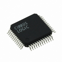
IC ANLG VOL CTRL 8CH DGTL 48LQFP
Manufacturer
Cirrus Logic Inc
Type
Controllerr
Datasheet
1.CS3308-CQZ.pdf
(44 pages)
Specifications of CS3308-CQZ
Package / Case
48-LQFP
Applications
High End Audio
Mounting Type
Surface Mount
Product
General Purpose Audio Amplifiers
Output Power
362 mW
Available Set Gain
22 dB
Thd Plus Noise
- 112 dB
Operating Supply Voltage
3.5 V / 5.25 V
Supply Current
36 mA
Maximum Operating Temperature
+ 70 C
Mounting Style
SMD/SMT
Audio Load Resistance
2 KOhms
Input Offset Voltage
0.75 V
Input Signal Type
Single
Minimum Operating Temperature
- 10 C
Output Signal Type
Analog
Supply Voltage (max)
5.25 V
Supply Voltage (min)
3.1 V
Output Type
8-Channel Audio
Lead Free Status / RoHS Status
Lead free / RoHS Compliant
For Use With
598-1778 - EVALUATION BOARD FOR CS5376598-1496 - BOARD EVAL FOR CS3308 VOL CTRL
Lead Free Status / Rohs Status
Lead free / RoHS Compliant
Other names
598-1598
Available stocks
Company
Part Number
Manufacturer
Quantity
Price

Company:
Part Number:
CS3308-CQZR
Manufacturer:
Cirrus Logic Inc
Quantity:
10 000


28
5.9.2
SCL
SDA
Since the read operation cannot set the MAP, an aborted write operation is used as a preamble. As shown
in
dition.
SPI Mode
In SPI Mode, CS is the CS3308 chip-select signal, CCLK, is the control port bit clock (input into the
CS3308 from the microcontroller), and MOSI is the input data line from the microcontroller. Data is
clocked in on the rising edge of CCLK. The default chip address in SPI Mode is 1000000b.
Figure 14
first seven bits on MOSI form the chip address and must be either the Individual, Group 1, or Group 2 chip
address as set by their respective control port registers. The eighth bit is a read/write indicator (R/W),
which must be low to write. If the read/write indicator is set high (indicating a read operation), the CS3308
will ignore all traffic on the SPI bus until CS is brought high and then low again. The next eight bits form
the Memory Address Pointer (MAP), which is set to the address of the register that is to be written. The
next eight bits are the data which will be placed into the register designated by the MAP.
There is a MAP auto increment capability, enabled by the INCR bit (the MSB of the MAP byte). If INCR is
‘0’, the MAP will stay constant for successive read or writes. If INCR is ‘1’, the MAP will automatically in-
crement after each byte is written, allowing block writes of successive registers.
Referenced Control
Individual Address...............
Group 1 Address .................
Group 2 Address .................
Referenced Control
Individual Address...............
Group 1 Address .................
Group 2 Address .................
Figure
MOSI
CCLK
START
CS
MSB
13, the write operation is aborted after the acknowledge for the MAP byte by sending a stop con-
0
CHIP ADDRESS (WRITE)
shows the operation of the control port in SPI Mode. To write to a register, bring CS low. The
1
Chip Address
2
MSB
3
4
5
LSB
Chip Address
Register Location
Register Location
6
“Individual Chip Address 1Bh” on page 41
“Group 1 Chip Address 1Ah” on page 40
“Group 2 Chip Address 19h” on page 40
“Individual Chip Address 1Bh” on page 41
“Group 1 Chip Address 1Ah” on page 40
“Group 2 Chip Address 19h” on page 40
1 Byte
7
0
ACK
Figure 13. Control Port Timing, I²C Read
8
9
INCR
10 11
6
Figure 14. SPI Write Cycle
LSB
5
MAP BYTE
12 13 14 15
4
W
3
INCR
2
1
MSB
16
0
ACK
STOP
17 18
START
Memory Address Pointer
1 Byte
19
MSB
20 21 22 23 24
CHIP ADDRESS (READ)
Chip Address
LSB
LSB
25
26 27 28
MSB
1
ACK
7
DATA
0
ACK
> 1 Byte
Data
DATA +1
7
0
DATA + n
7
CS3308
0
LSB
ACK
NO
DS702F1
STOP
Related parts for CS3308-CQZ
Image
Part Number
Description
Manufacturer
Datasheet
Request
R

Part Number:
Description:
IC,Tone/Volume/Balance Control,QFP,48PIN,PLASTIC
Manufacturer:
Cirrus Logic Inc
Datasheet:

Part Number:
Description:
IC 8-Channel Digital Volume Control
Manufacturer:
Cirrus Logic Inc
Part Number:
Description:
Audio Amplifiers IC 8-Channel Digital Volume Control
Manufacturer:
Cirrus Logic Inc
Datasheet:

Part Number:
Description:
THIN FILM SFERNICE / CS 33 11K5 2% 0,5% E
Manufacturer:
Vishay
Part Number:
Description:
THIN FILM SFERNICE / CS 33 1M 1M 1% 0,5% R0016 E
Manufacturer:
Vishay
Part Number:
Description:
THIN FILM SFERNICE / CS 33 1M 500K 1% 0,5% E
Manufacturer:
Vishay
Part Number:
Description:
THIN FILM SFERNICE / CS 33 278K 222K 1% 1% E
Manufacturer:
Vishay

Part Number:
Description:
Dual Value Chip Resistors, Center Tap
Manufacturer:
Vishay Intertechnology
Datasheet:
Part Number:
Description:
Dual Value Chip Resistors, Center Tap
Manufacturer:
VISHAY [Vishay Siliconix]
Datasheet: