AD532KH Analog Devices Inc, AD532KH Datasheet
AD532KH
Specifications of AD532KH
Available stocks


Related parts for AD532KH


AD532KH Summary of contents
Page 1
FEATURES Pretrimmed to ±1.0% (AD532K) No external components required Guaranteed ±1.0% maximum 4-quadrant error (AD532K) Differential Inputs for (X − − function Monolithic construction, low cost APPLICATIONS Multiplication, division, squaring, square rooting ...
Page 2
AD532 TABLE OF CONTENTS Features .............................................................................................. 1 Applications ....................................................................................... 1 Functional Block Diagram .............................................................. 1 General Description ......................................................................... 1 Flexibility of Operation................................................................ 1 Guaranteed Performance Over Temperature ........................... 1 Advantages of On-The-Chip Trimming of The Monolithic AD532 ............................................................................................ 1 Revision ...
Page 3
SPECIFICATIONS At 25° ± ≥ 2 kΩ V grounded, unless otherwise noted Table 1. Conditions Model MULTIPLIER PERFORMANCE Transfer Function Total Error –10 V ≤ ≤ + Minimum to ...
Page 4
AD532 Model Conditions SQUARE PERFORMANCE Transfer Function Total Error SQUARE ROOTER PERFORMANCE Transfer Function Total Error 0 V ≤ POWER SUPPLY SPECIFICATIONS Supply Voltage Rated Performance Operating Supply Current Quiescent AD532J Min Typ Max − ...
Page 5
THERMAL RESISTANCE θ is specified for the worst-case conditions, that is, a device JA soldered in a circuit board for surface-mount packages. Table 2. Thermal Resistance Package Type θ JA H-10A 150 E-20A 85 D-14 85 CHIP DIMENSIONS AND BONDING ...
Page 6
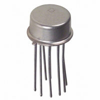
AD532 PIN CONFIGURATION AND FUNCTION DESCRIPTIONS Table 3. 10 Lead Header Pin Function Descriptions Pin No. Mnemonic OUT 5 − GND 9 V ...
Page 7
Table 4. 20 Lead Leadless Chip Carrier Pin Function Descriptions Pin No. Mnemonic OUT 4 − 11, 12 GND 16 ...
Page 8
AD532 TYPICAL PERFORMANCE CHARACTERISTICS 0.1 0. PEAK SIGNAL AMPLITUDE (V) Figure 6. Distortion vs. Peak Signal Amplitude 100 20V p-p SIGNAL 10 1 0.1 10 100 1k 10k ...
Page 9
SATURATED OUTPUT SWING 10 MAX INPUT FOR 1% LINEARITY POWER SUPPLY VOLTAGE (V) Figure 12. Signal Swing vs. Supply ...
Page 10
AD532 FUNCTIONAL DESCRIPTION The functional block diagram for the AD532 is shown in Figure 1and the complete schematic in Figure 14. In the multiplying and squaring modes connected to the output to close the feedback around the output ...
Page 11
AD532 PERFORMANCE CHARACTERISTICS Multiplication accuracy is defined in terms of total error at 25°C with the rated power supply. The value specified is in percent of full scale and includes X and Y nonlinearities, feedback and IN IN scale factor ...
Page 12
AD532 APPLICATIONS The performance and ease of use of the AD532 is achieved through the laser trimming of thin-film resistors deposited directly on the monolithic chip. This trimming-on-the-chip technique provides a number of significant advantages in terms of cost, reliability ...
Page 13
Table 6. Adjustment Procedure (Divider or Square Rooter) Divider With: Adjust for: Adjust OUT Scale Factor −10 V +10 V − (Offset) −1 V +0.1 V − Repeat if required. SQUARE ROOT Z ...
Page 14
AD532 OUTLINE DIMENSIONS 0.358 (9.09) 0.342 (8.69) CONTROLLING DIMENSIONS ARE IN INCHES; MILLIMETER DIMENSIONS (IN PARENTHESES) ARE ROUNDED-OFF INCH EQUIVALENTS FOR REFERENCE ONLY AND ARE NOT APPROPRIATE FOR USE IN DESIGN. 0.185 (4.70) 0.165 (4.19) 0.040 (1.02) MAX 0.050 (1.27) ...
Page 15
... AD532JHZ 0°C to 70°C AD532KD 0°C to 70°C AD532KDZ 0°C to 70°C AD532KH 0°C to 70°C AD532KHZ 0°C to 70°C AD532SCHIPS −55°C to +125°C AD532SD −55°C to +125°C AD532SD/883B −55°C to +125°C AD532SE/883B −55°C to +125°C AD532SH − ...
Page 16
AD532 NOTES ©2001–2011 Analog Devices, Inc. All rights reserved. Trademarks and registered trademarks are the property of their respective owners. D00502-0-2/11(D) Rev Page ...