EL9202ILZ Intersil, EL9202ILZ Datasheet
EL9202ILZ
Specifications of EL9202ILZ


Related parts for EL9202ILZ

EL9202ILZ Summary of contents
Page 1
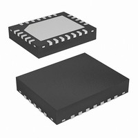
... VOUTB NC 4 PAD VINB- VIND+ 5 SET AVDD 6 CE CTL 7 | Intersil (and design registered trademark of Intersil Americas Inc. Copyright Intersil Americas Inc. 2005, 2008. All Rights Reserved All other trademarks mentioned are the property of their respective owners. 19 VOUTB 18 VOUTC 17 VINC VINC+ 14 GND ...
Page 2
... EL9202ILZ (Note) 9202ILZ EL9202ILZ-T7* (Note) 9202ILZ EL9202ILZ-T13* (Note) 9202ILZ *Add “-T” suffix for tape and reel *Please refer to TB347 for details on reel specifications. NOTE: These Intersil Pb-free plastic packaged products employ special Pb-free material sets, molding compounds/die attach materials, and 100% matte tin plate plus anneal (e3 termination finish, which is RoHS compliant and compatible with both SnPb and Pb-free soldering operations) ...
Page 3
... EE EE Write Cycles WC 3 EL9200, EL9201, EL9202 Thermal Information = +25°C) A Maximum Die Temperature . . . . . . . . . . . . . . . . . . . . . . . . . . +150°C Storage Temperature . . . . . . . . . . . . . . . . . . . . . . . .-65°C to +150°C Pb-Free Reflow Profile .see link below http://www.intersil.com/pbfree/Pb-FreeReflow.asp Operating Conditions Ambient Operating Temperature . . . . . . . . . . . . . . . .-40°C to +85° 15V 15V 24.9kΩ, and T ...
Page 4
Electrical Specifications PARAMETER DESCRIPTION SET SET Differential Nonlinearity DN SET SET Zero-Scale Error ZSE SET SET Full-Scale Error FSE I SET Current SET SET SET External Resistance SET A to SET Voltage ...
Page 5
Pin Descriptions PIN IN/OUT VINx- Input VINx+ Input VS+ Supply VOUTX Output NC - GND Supply IOUT Output SET Output CE Input CTL Input AVDD Supply VSD Supply 5 EL9200, EL9201, EL9202 DESCRIPTION Amplifier x inverting input, where ...
Page 6
Amplifier Typical Performance Curves 500 +25°C A 400 300 200 100 0 INPUT OFFSET VOLTAGE (mV) FIGURE 1. INPUT OFFSET VOLTAGE DISTRIBUTION 5.0 0 INPUT OFFSET ...
Page 7
Amplifier Typical Performance Curves -50 - TEMPERATURE (°C) FIGURE 7. OPEN-LOOP GAIN vs TEMPERATURE 0 -0.02 -0.04 -0.06 -0.08 -0.10 -0.12 -0.14 -0.16 -0.18 0 100 IRE FIGURE 9. DIFFERENTIAL GAIN - ...
Page 8
Amplifier Typical Performance Curves 0pF 3 LOAD 1 -1 150Ω 100k 1M FREQUENCY (Hz) FIGURE 13. FREQUENCY RESPONSE FOR VARIOUS R 400 350 300 250 200 150 ...
Page 9
Amplifier Typical Performance Curves 1k 100 10 1 100 1k 10k 100k FREQUENCY (Hz) FIGURE 19. INPUT VOLTAGE NOISE SPECTRAL DENSITY 100 1kΩ 50mV IN T ...
Page 10
Amplifier Typical Performance Curves JEDEC JESD51-7 HIGH EFFECTIVE THERMAL CONDUCTIVITY TEST BOARD - QFN EXPOSED DIEPAD SOLDERED TO PCB PER JESD51-5 4.5 4.0 3.378W 3.5 3.0 2.5 2.0 1.5 1.0 0 AMBIENT TEMPERATURE (°C) ...
Page 11
The output sink current will decrease and the V level will increase by one LSB. COM To avoid unintentional adjustment, the EL9200, EL9201, and EL9202 guarantees to reject CTL pulses shorter than 20µs. INPUT CTL CE Mid ...
Page 12
Non-Volatile Memory (EEPROM) Programming When the CTL pin exceeds 4.9V, the non-volatile programming cycle will be activated. The CTL signal needs to remain above 4.9V for more than 200µs. The level and timing needed to program the non-volatile memory is ...
Page 13
... Accordingly, the reader is cautioned to verify that data sheets are current before placing orders. Information furnished by Intersil is believed to be accurate and reliable. However, no responsibility is assumed by Intersil or its subsidiaries for its use; nor for any infringements of patents or other rights of third parties which may result from its use ...
Page 14
QFN (Quad Flat No-Lead) Package Family PIN #1 3 I.D. MARK 2X 0.075 C TOP VIEW 0. (E2) 7 (D2) BOTTOM VIEW 0. SEATING PLANE 0.08 C ...
Page 15
Package Outline Drawing L12.4x4B 12 LEAD DUAL FLAT NO-LEAD PLASTIC PACKAGE Rev 0, 06/08 4.00 6 PIN 1 INDEX AREA (4X) 0.15 TOP VIEW ( 3.20) 3.65 ( 10X TYPICAL RECOMMENDED LAND PATTERN 15 EL9200, EL9201, ...