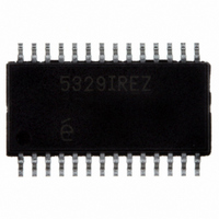
EL5329IREZ Intersil, EL5329IREZ Datasheet - Page 10

EL5329IREZ
Manufacturer Part Number
EL5329IREZ
Description
IC BUFFER GAMMA 10-CHAN 28HTSSOP
Manufacturer
Intersil
Datasheet
1.EL5329IREZ.pdf
(13 pages)
Specifications of EL5329IREZ
Applications
TFT-LCD Panels: Gamma Buffer, VCOM Driver
Output Type
Rail-to-Rail
Number Of Circuits
10
-3db Bandwidth
10MHz
Slew Rate
9 V/µs
Current - Supply
5.5mA
Current - Output / Channel
120mA
Voltage - Supply, Single/dual (±)
4.5 V ~ 16.5 V, ±2.25 V ~ 8.25 V
Mounting Type
Surface Mount
Package / Case
28-TSSOP Exposed Pad, 28-eTSSOP, 28-HTSSOP
Lead Free Status / RoHS Status
Lead free / RoHS Compliant
Available stocks
Company
Part Number
Manufacturer
Quantity
Price
Part Number:
EL5329IREZ
Manufacturer:
ELANTEC
Quantity:
20 000
Description of Operation and Application
Information
Product Description
The EL5129 and EL5329 are fabricated using a high voltage
CMOS process. They exhibit rail to rail input and output
capability and have very low power consumption. When
driving a load of 10K and 12pF, the buffers have a
-3dB bandwidth of 10MHz and exhibit 9V/µs slew rate. The
V
10V/µs slew rate.
Input, Output, and Supply Voltage Range
The EL5129 and EL5329 are specified with a single nominal
supply voltage from 5V to 15V or a split supply with its total
range from 5V to 15V. Correct operation is guaranteed for a
supply range from 4.5V to 16.5V.
The input common-mode voltage range of the EL5129 and
EL5329 within 500mV beyond the supply rails. The output
swings of the buffers and V
within 100mV of the positive and negative supply rails with
load currents of 5mA. Decreasing load currents will extend
the output voltage even closer to each supply rails.
Output Phase Reversal
The EL5129 and EL5329 are immune to phase reversal as
long as the input voltage is limited from V
+0.5V. Although the device's output will not change phase,
the input's over-voltage should be avoided. If an input
voltage exceeds supply voltage by more than 0.6V,
electrostatic protection diode placed in the input stage of the
device begin to conduct and over-voltage damage could
occur.
Output Drive Capability
The EL5129 and EL5329 do not have internal short-circuit
protection circuitry. The buffers will limit the short circuit
current to ±120mA and the V
circuit current to ±170mA if the outputs are directly shorted
to the positive or the negative supply. If the output is shorted
indefinitely, the power dissipation could easily increase such
that the part will be destroyed. Maximum reliability is
maintained if the output continuous current never exceeds
±15mA for the buffers and ±100mA for the V
These limits are set by the design of the internal metal
interconnections.
The Unused Buffers
It is recommended that any unused buffers should have their
inputs tied to ground plane.
Power Dissipation
With the high-output drive capability of the EL5129 and
EL5329, it is possible to exceed the 125°C “absolute-
maximum junction temperature” under certain load current
conditions. Therefore, it is important to calculate the
COM
amplifier has a -3dB bandwidth of 12MHz and exhibit
COM
COM
10
amplifier typically extend to
amplifier will limit the short
S
- -0.5V to V
COM
amplifier.
EL5129, EL5329
S
+
maximum junction temperature for the application to
determine if load conditions need to be modified for the
buffer to remain in the safe operating area.
The maximum power dissipation allowed in a package is
determined according to:
where:
• T
• T
• θ
• P
The maximum power dissipation actually produced by an IC
is the total quiescent supply current times the total power
supply voltage, plus the power in the IC due to the loads, or:
P
(
when sourcing, and:
P
(
when sinking.
where:
• i = 1 to total number of buffers
• V
• I
• V
• V
• I
• I
If we set the two P
can solve for the R
package power dissipation curves provide a convenient way
to see if the device will overheat. The maximum safe power
dissipation can be found graphically, based on the package
type and the ambient temperature. By using the previous
equation, it is a simple matter to see if P
device's power derating curves.
P
V
V
DMAX
DMAX
DMAX
S
OUT
SMAX
LOAD
LA
JA
AMAX
+
JMAX
DMAX
S
OUT
OUT
–
= Total supply voltage of buffer and V
= Load current of V
= Thermal resistance of the package
–
V
=
=
=
i = Maximum output voltage of the application
OUT
V
i = Load current of buffer
= Maximum output voltage of V
= Total quiescent current
= Maximum junction temperature
= Maximum ambient temperature
S
V
V
T
-------------------------------------------- -
= Maximum power dissipation in the package
- )
JMAX
S
S
)
×
×
×
×
I
I
I
I
S
S
LA
Θ
LA
+
+
- T
JA
DMAX
Σi
Σi
LOAD
AMAX
×
×
( [
[
(
V
V
's to avoid device overheat. The
equations equal to each other, we
COM
S
OUT
+
–
i
V
–
OUT
V
S
- )
i )
×
×
I
I
LOAD
COM
DMAX
LOAD
COM
i ]
i ]
exceeds the
+
+
May 13, 2005
FN7430.1


