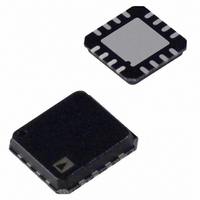
ADD8704ACPZ-R2 Analog Devices Inc, ADD8704ACPZ-R2 Datasheet - Page 12

ADD8704ACPZ-R2
Manufacturer Part Number
ADD8704ACPZ-R2
Description
IC OPAMP LCD QUAD 16V 16LFCSP
Manufacturer
Analog Devices Inc
Datasheet
1.ADD8704ACPZ-R2.pdf
(16 pages)
Specifications of ADD8704ACPZ-R2
Applications
TFT-LCD Panels: Gamma Buffer, VCOM Driver
Number Of Circuits
4
-3db Bandwidth
6.8MHz
Slew Rate
6 V/µs
Current - Supply
2.8mA
Current - Output / Channel
35mA
Voltage - Supply, Single/dual (±)
4.5 V ~ 16 V
Mounting Type
Surface Mount
Package / Case
16-LFCSP
Lead Free Status / RoHS Status
Lead free / RoHS Compliant
ADD8704
APPLICATION INFORMATION
THEORY
The ADD8704 is designed for use in LCD gamma correction
circuits. Depending on the panel architecture, between 4 and 18
different gamma voltages may be needed. These gamma
voltages provide the reference voltages for the column driver
RDACs. Due to the capacitive nature of LCD panels, it is
necessary for these drivers to provide high capacitive load drive.
In addition to providing gamma reference voltages, these parts
are also capable of providing the V
center voltage common to all the LCD pixels. Since the V
circuit is common to all the pixels in the panel, the V
is designed to supply continuous currents up to 35 mA.
INPUT
The ADD8704 has four amplifiers specifically designed for the
needs of an LCD panel. F
correction curve for a normally white twisted nematic LCD
panel. The symmetric curve comes from the need to reverse the
polarity on the LC pixels to avoid “burning” in the image. The
application therefore requires gamma voltages that come close
to both supply rails. To accommodate this transfer function, the
ADD8704 has been designed to have four different amplifiers in
one package.
Amplifier A has a single-supply PNP input stage followed by a
folded cascode stage. This provides an input range that goes to
the bottom rail. This amplifier can therefore be used to provide
the bottom voltage on the RDAC string.
Amplifier B (PNP folded cascode) swings to the low rail as well,
but it provides 35 mA continuous output current versus 15 mA.
This buffer is suitable for lower RDAC range, middle RDAC
range, or V
V
V
V
V
V
V
V
V
V
V
V
V
G10
DD
G1
G2
G3
G4
G5
G6
G7
G8
G9
SS
0
COM
applications.
Figure 36. LCD Gamma Correction Curve
16
igure 36
GRAY SCALE BITS
32
shows a typical gamma
COM
voltage. V
48
COM
is the
COM
64
driver
COM
Rev. 0 | Page 12 of 16
Amplifier C is a rail-to-rail input range that makes the
ADD8704 suitable for use anywhere on the RDAC as well as for
V
Amplifier D has an NPN follower input stage. This covers the
upper rail to GND plus 1.7 V. This amplifier is suitable for the
upper range of the RDAC.
OUTPUT
The outputs of the amplifiers have been designed to match the
performance needs of the gamma correction circuit. All four of
the amplifiers have rail-to-rail outputs, but the current drive
capabilities differ. Since amplifier A is suited for voltages close
to V
it sources; it can sink 15 mA of continuous current. Likewise,
since amplifier D is primarily used for voltages close to V
sources more current. Amplifier D can source 15 mA of
continuous current. Amplifiers B and C are designed for use as
either midrange gamma or V
and source equal amounts of current. Since they are used as
V
continuous current.
The nature of LCD panels introduces a large amount of
parasitic capacitance from the column drivers as well as the
capacitance associated with the liquid crystals via the common
plane. This makes capacitive drive capability an important
factor when designing the gamma correction circuit.
IMPORTANT NOTE
Because of the asymmetric nature of amplifiers A and D, care
must be taken to connect an input that forces the amplifiers to
operate in their most productive output states. Amplifier D has
very limited sink capabilities, while amplifier A does not source
well. If more than one ADD8704 is used, set the amplifier D
input to enable the amplifier output to source current and set
the amplifier A input to force a sinking output current. This
means making sure the input is above the midpoint of the
common-mode input range for amplifier D and below the
midpoint for amplifier A. Mathematically speaking, make sure
V
Figure 37 shows an example using 4 ADD8704s to generate 10
gamma outputs. Note that the top three resistor tap-points are
connected to the amplifier D inputs, thus assuring these
channels will source current. Likewise, the bottom three resistor
tap-points are connected to the amplifier A inputs to provide
sinking output currents.
COM
COM
IN
> V
SS
applications.
amplifiers, they have a drive capability of up to 35 mA of
(GND), the output is designed to sink more current than
S
/2 for amplifier D and V
COM
IN
amplifiers. They therefore sink
< V
S
/2 for amplifier A.
DD
, it


