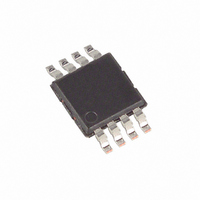
MAX9584AUA+ Maxim Integrated Products, MAX9584AUA+ Datasheet - Page 8

MAX9584AUA+
Manufacturer Part Number
MAX9584AUA+
Description
IC AMP VIDEO FILTER 8-UMAX
Manufacturer
Maxim Integrated Products
Datasheet
1.MAX9583AZTT.pdf
(15 pages)
Specifications of MAX9584AUA+
Applications
Filter
Number Of Circuits
3
Current - Supply
3.5mA
Current - Output / Channel
140mA
Voltage - Supply, Single/dual (±)
2.7 V ~ 3.6 V
Mounting Type
Surface Mount
Package / Case
8-TSSOP, 8-MSOP (0.118", 3.00mm Width)
Lead Free Status / RoHS Status
Lead free / RoHS Compliant
Dual, Triple, and Quad Standard-Definition Video
Filter Amplifiers with DC-Coupled Input Buffers
The MAX9583/MAX9584/MAX9585 filter and amplify the
video DAC output in applications such as set-top boxes
and televisions. These devices consist of input buffers,
lowpass filters, and gain of 2V/V output amplifiers capa-
ble of driving a standard 150Ω video load to ground.
The video inputs should be directly connected to the
output of the video current DAC. DC coupling ensures
that the input signals are ground referenced so that the
sync tip of composite or luma signals is within 50mV of
ground and the blank level of the chroma signal is
between 0.5V and 0.65V. Since the input buffers are
identical, any standard-definition video signal can be
applied to those inputs provided the signal is between
ground and 1.05V when V
three composite video signals could be applied to INA,
INB, and INC of the MAX9584. The RGB set or the
YPbPr set can also be inputs to INA, INB, and INC of
the MAX9584.
The filter passband (±1dB) is typically 8.5MHz, which
makes the device suitable for standard-definition video
signals from all sources (e.g., broadcast and DVD).
Broadcast video signals are channel limited: NTSC sig-
nals have 4.2MHz bandwidth and PAL signals have
5MHz bandwidth. Video signals from a DVD player,
however, are not channel limited, so the bandwidth of
DVD video signals can approach the Nyquist limit of
6.75MHz. (Recommendation ITU-R BT.601-5 specifies
13.5MHz as the sampling rate for standard-definition
video). Therefore, the maximum bandwidth of the signal
is 6.75MHz. To ease the filtering requirements, most
modern video systems oversample by two times, clock-
ing the video current DAC at 27MHz.
The video output amplifiers can both source and sink
load current, allowing output loads to be DC- or AC-
coupled. The amplifier output stage needs approxi-
mately 300mV of headroom from either supply rail. The
devices have an internal level-shift circuit that positions
the sync tip at approximately 300mV at the output. The
blank level of the chroma output is positioned at
approximately 1.3V if the blank level of the chroma
input signal is 0.5V. The blank level of the chroma out-
put is positioned at approximately 1.5V if the blank level
of the chroma input signal is 0.6V.
8
_______________________________________________________________________________________
Detailed Description
DD
= 2.7V. For example,
Video Filter
Outputs
Inputs
If the supply voltage is greater than 3.135V (5% below
a 3.3V supply), each amplifier can drive two DC-cou-
pled video loads to ground. If the supply is less than
3.135V, each amplifier can drive only one DC-coupled
or AC-coupled video load.
The MAX9583/MAX9584/MAX9585 have high-imped-
ance input buffers that work with source resistances as
high as 1000Ω. To reduce power dissipation in the
video DACs, the DAC output resistor can be scaled up
in value. The reference resistor that sets the reference
current inside the video DACs must also be similarly
scaled up. For instance, if the output resistor is 37.5Ω,
the DAC must source 26.7mA when the output is 1V. If
the output resistor is increased to 300Ω, then the DAC
only needs to source 3.33mA when the output is 1V.
There is parasitic capacitance from the DAC output to
ground. That capacitance, in parallel with the DAC out-
put resistor, forms a pole that can potentially roll off the
frequency response of the video signal. For example,
300Ω in parallel with 50pF create a pole at 10.6MHz. To
minimize this capacitance, reduce the area of the sig-
nal trace attached to the DAC output as much as possi-
ble, and place the MAX9583/MAX9584/MAX9585 as
close as possible to the video DAC outputs.
The outputs can be AC-coupled since the output stage
can source and sink current as shown in Figure 1.
Coupling capacitors should be 220µF or greater to
keep the highpass filter, formed by the 150Ω equivalent
resistance of the video transmission line, to a corner
frequency of 4.8Hz or below. The frame rate of PAL
systems is 25Hz, and the frame rate of NTSC systems
is 30Hz. The corner frequency should be well below the
frame rate.
The MAX9583/MAX9584/MAX9585 operate from a single-
supply voltage down to 2.7V, allowing for low-power opera-
tion. Bypass V
external components as close as possible to the device.
Power-Supply Bypassing and Ground
DD
Applications Information
Reducing Power Consumption
to GND with a 0.1µF capacitor. Place all
AC-Coupling the Outputs
in the Video DACs


