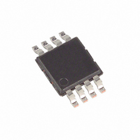
MAX9551EUA+T Maxim Integrated Products, MAX9551EUA+T Datasheet - Page 2

MAX9551EUA+T
Manufacturer Part Number
MAX9551EUA+T
Description
IC BUFFER VCOM 8-UMAX
Manufacturer
Maxim Integrated Products
Datasheet
1.MAX9551EUA.pdf
(12 pages)
Specifications of MAX9551EUA+T
Applications
TFT-LCD Panels: VCOM Driver
Number Of Circuits
2
Current - Supply
2mA
Current - Output / Channel
55mA
Voltage - Supply, Single/dual (±)
6 V ~ 20 V, ±3 V ~ 10 V
Mounting Type
Surface Mount
Package / Case
8-TSSOP, 8-MSOP (0.118", 3.00mm Width), Exposed Pad
Operating Supply Voltage
7 V to 20 V
Maximum Power Dissipation
824.7 mW
Maximum Operating Temperature
+ 85 C
Minimum Operating Temperature
- 40 C
Lead Free Status / RoHS Status
Lead free / RoHS Compliant
ABSOLUTE MAXIMUM RATINGS
Supply Voltage (V
Any Other Pin to GND ................................-0.3V to (V
IN+/IN- (current) ...............................................................±20mA
OUT, OUT_ (current)................................................................1A
Continuous Power Dissipation (T
High-Current VCOM Drive Buffers
for TFT LCDs
ELECTRICAL CHARACTERISTICS
(V
T
Stresses beyond those listed under “Absolute Maximum Ratings” may cause permanent damage to the device. These are stress ratings only, and functional
operation of the device at these or any other conditions beyond those indicated in the operational sections of the specifications is not implied. Exposure to
absolute maximum rating conditions for extended periods may affect device reliability.
2
DC CHARACTERISTICS
Supply Voltage Range
Quiescent Current
Low Output Voltage
High Output Voltage
Input Offset Voltage
Input Bias Current
Input Resistance
Common-Mode Input Voltage
Common-Mode Rejection Ratio
Power-Supply Rejection Ratio
Continuous Output Current
Output Load Regulation
Output Load Regulation
Thermal Shutdown
Thermal Hysteresis
A
5-Pin Thin SOT23 (derate 2.7mW/°C above +70°C) ...219.1mW
DD
= +25°C.) (Note 1)
_______________________________________________________________________________________
= 16V, GND = 0V, V
PARAMETER
DD
to GND) ................................-0.3V to +22V
CM
= V
A
= +70°C)
OUT
SYMBOL
CMRR
CMVR
PSRR
V
V
V
LR1
LR2
V
I
R
= V
CC
I
I
DD
OH
OL
OS
O
B
IN
DD
/ 2, C
Inferred from PSRR test and transient
load test
Per channel
I
I
Inferred from CMRR
2V ≤ V
V
V
load, regulation test
I
I
V
V
L
H
OUT
OUT
OUT
DD
DD
OUT
= -4mA
= +4mA
DD
L
= 7V, V
= 7V,
= 0mA to 50mA
= 0mA to -50mA
= 3.5V, V
= 3.5V
IN
+ 0.3V)
= 1µF, T
≤ (V
OUT
DD
CONDITIONS
DD
A
- 2V)
= 3.5V, guaranteed by
= T
= 7V to 16V
Operating Temperature Range ...........................-40°C to +85°C
Junction Temperature ......................................................+150°C
Storage Temperature Range .............................-65°C to +150°C
Lead Temperature (soldering, 10s) .................................+300°C
I
I
OUT
OUT
MIN
8-Pin µMAX (derate 10.3mW/°C above +70°C) ........824.7mW
14-Pin TSSOP (derate 20.8mW/°C above +70°C) .....1667mW
= 0mA to -55mA
= 0mA to 55mA
to T
MAX
, unless otherwise noted. Typical values are at
MIN
-10
80
80
55
7
2
V
DD
+160
TYP
0.04
0.01
6.5
6.5
+1
96
96
15
2
- 0.04
1
6
6
V
V
DD
MAX
DD
+10
0.1
20
13
13
15
15
4
1
- 0.1
- 2
UNITS
MΩ
mA
mV
mA
mV
mV
dB
dB
µA
°C
°C
V
V
V
V


