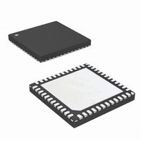
ISL59483IRZ-T13 Intersil, ISL59483IRZ-T13 Datasheet - Page 13

ISL59483IRZ-T13
Manufacturer Part Number
ISL59483IRZ-T13
Description
IC MUX AMP DUAL 500MHZ 48-QFN
Manufacturer
Intersil
Datasheet
1.ISL59483IRZ.pdf
(17 pages)
Specifications of ISL59483IRZ-T13
Applications
4:1 Multiplexer-Amplifier
Number Of Circuits
3
-3db Bandwidth
500MHz
Slew Rate
1600 V/µs
Current - Supply
92mA
Current - Output / Channel
125mA
Mounting Type
Surface Mount
Package / Case
48-VQFN
Lead Free Status / RoHS Status
Lead free / RoHS Compliant
Pin Equivalent Circuits
AC Test Circuits
Figure 42A illustrates the optimum output load for testing AC
performance. Figure 42B illustrates the optimum output load
when connecting to 50Ω input terminated equipment.
FIGURE 42B. TEST CIRCUIT FOR MEASURING WITH 50Ω OR
FIGURE 42C. BACKLOADED TEST CIRCUIT FOR VIDEO
FIGURE 42A. TEST CIRCUIT WITH OPTIMAL OUTPUT LOAD
V
V
IN
IN
50Ω
75Ω
50Ω
75Ω
or
or
GNDC1
GNDB1
GNDA1
V1+
IN
ISL59483
ISL59483
V1-
75Ω INPUT TERMINATED EQUIPMENT
CABLE APPLICATION. BANDWIDTH AND
LINEARITY FOR R
DEGRADED.
V
IN
50Ω
75Ω
or
FIGURE 42. TEST CIRCUITS
CIRCUIT 4A
C
5pF
C
5pF
L
L
CIRCUIT 1
ISL59483
475Ω
50Ω or 75Ω
R
R
S
S
13
CAPACITIVELY
COUPLED
ESD CLAMP
L
C
5pF
L
50Ω
75Ω
LESS THAN 500Ω WILL BE
or
V+
V-
500Ω
R
L
GNDB2
GNDA2
GNDC2
LOGIC PIN
EQUIPMENT
EQUIPMENT
50Ω
75Ω
50Ω
75Ω
V2+
or
V2-
or
TEST
TEST
CIRCUIT 4B
ISL59483
21k
33k
CIRCUIT 2
1.2V
CAPACITIVELY
COUPLED
ESD CLAMP
+
Application Information
General
The ISL59483 is ideal as the matrix element of high
performance switchers and routers. Key features include
high impedance buffered analog inputs and excellent AC
performance at output loads down to 150Ω for video cable-
driving. The current feedback output amplifiers are stable
operating into capacitive loads and bandwidth is optimized
with a load of 5pF in parallel with a 500Ω. Total output
capacitance can be split between the PCB capacitance and
an external load capacitor.
Ground Connections
For the best isolation and crosstalk rejection, all GND pins
must connect to the GND plane.
Power-up Considerations
The ESD protection circuits use internal diodes from all pins
the V+ and V- supplies. In addition, a dV/dT-triggered clamp
is connected between the V+ and V- pins, as shown in the
Equivalent Circuits 1 through 4 section of the Pin Description
table. The dV/dT triggered clamp imposes a maximum
supply turn-on slew rate of 1V/µs. Damaging currents can
flow for power supply rates-of-rise in excess of 1V/µs, such
as during hot plugging. Under these conditions, additional
methods should be employed to ensure the rate of rise is not
exceeded.
Consideration must be given to the order in which power is
applied to the V+ and V- pins, as well as analog and logic
input pins. Schottky diodes (Motorola MBR0550T or
equivalent) connected from V+ to ground and V- to ground
(Figure 43) will shunt damaging currents away from the
internal V+ and V- ESD diodes in the event that the V+
supply is applied to the device before the V- supply. One
Schottky can be used to protect both V+ power supply pins,
and a second for the protection of both V- pins.
-
GND
V+
V-
V1-
SUBSTRATE 1
~1M
Ω
THERMAL HEAT SINK PAD
CIRCUIT 3
SUBSTRATE 2
V-
V+
OUT
~1M
Ω
May 21, 2007
FN6394.2
V2-


