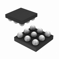
ISL59123IIZ-T7 Intersil, ISL59123IIZ-T7 Datasheet - Page 9

ISL59123IIZ-T7
Manufacturer Part Number
ISL59123IIZ-T7
Description
IC VIDEO DRVR TRI-CHN LPF 9WLCSP
Manufacturer
Intersil
Datasheet
1.ISL59123IIZ-T7.pdf
(10 pages)
Specifications of ISL59123IIZ-T7
Applications
Reconstruction Filter
Output Type
Rail-to-Rail
Number Of Circuits
3
-3db Bandwidth
18MHz
Slew Rate
60 V/µs
Current - Supply
4mA
Current - Output / Channel
200mA
Voltage - Supply, Single/dual (±)
2.5 V ~ 3.6 V
Mounting Type
Surface Mount
Package / Case
9-WLCSP
Lead Free Status / RoHS Status
Lead free / RoHS Compliant
Application Information
The ISL59123 is a single-supply rail-to-rail triple video low-
pass filter and amplifier with a -3dB bandwidth of 18MHz. It
provides anti-aliasing for component, s-video, and
composite video signals. Its small size and low power make
the ISL59123 ideal for portable video applications.
The Sallen Key Low Pass Filter
The Sallen Key is a classic low pass configuration. This
provides a very stable low pass function, and in the case of
the ISL59123, a three-pole roll-off at 18MHz. The three-pole
function is accomplished with an RC low pass network placed
in series with and before the Sallen Key. The first pole is
formed by an RC network (including the impedance of the
source driving the ISL59123), with poles two and three
generated by a Sallen Key, creating a three-pole roll-off
characteristic at 18MHz.
Output Coupling
The ISL59123 can be AC or DC coupled to its output. When
AC coupled, a 220µF coupling capacitor is recommended to
ensure that low frequencies are passed, preventing video
“tilt” or “droop” across a line.
Output Drive Capability
The ISL59123 does not have internal short circuit protection
circuitry. If the output is shorted indefinitely, the power
dissipation could easily overheat the die or the current could
eventually compromise metal integrity. Maximum reliability is
maintained if the output current never exceeds ±40mA. This
limit is set by the design of the internal metal interconnect. Note
that for transient short circuits, the part is robust.
Short circuit protection can be provided externally with a back
match resistor in series with the output placed close as possible
to the output pin. In video applications this would be a 75Ω
resistor and will provide adequate short circuit protection to the
device. Care should still be taken not to stress the device with a
short at the output.
Power Dissipation
With the high output drive capability of the ISL59123, it is
possible to exceed the +125°C absolute maximum junction
temperature under certain load current conditions.
Therefore, it is important to calculate the maximum junction
temperature for an application to determine if load conditions
or package types need to be modified to assure operation of
the amplifier in a safe operating area.
The maximum power dissipation allowed in a package is
determined according to Equation 1:
PD
MAX
=
T
-------------------------------------------- -
JMAX
θ
–
JA
T
AMAX
9
(EQ. 1)
ISL59123
Where:
The maximum power dissipation actually produced by an IC
is the total quiescent supply current times the total power
supply voltage, plus the power in the IC due to the load, or:
for sourcing use Equation 2:
for sinking use Equation 3:
Where:
Power Supply Bypassing Printed Circuit Board
Layout
As with any modern operational amplifier, a good printed
circuit board layout is necessary for optimum performance.
Lead lengths should be as short as possible. The power
supply pin must be well bypassed to reduce the risk of
oscillation. For normal single supply operation, a single
4.7µF tantalum capacitor in parallel with a 0.1µF ceramic
capacitor from V
Printed Circuit Board Layout
For good AC performance, parasitic capacitance should be
kept to minimum. Use of wire wound resistors should be
avoided because of their additional series inductance. Use
of sockets should also be avoided if possible. Sockets add
parasitic inductance and capacitance that can result in
compromised performance.
PD
PD
T
T
θ
V
I
V
R
I
SMAX
LOAD
JA
AMAX
JMAX
MAX
MAX
S
OUT
LOAD
= Supply voltage
= Thermal resistance of the package
= Maximum output voltage of the application
=
=
= Load current
= Maximum quiescent supply current
= Maximum junction temperature
= Maximum ambient temperature
= Load resistance tied to ground
V
V
S
S
×
×
I
I
SMAX
SMAX
DD
to GND will suffice.
+
+
(
(
V
V
S
OUT
–
V
–
OUT
V
S
)
)
×
×
V
--------------- -
I
LOAD
OUT
R
L
April 4, 2007
FN6432.1
(EQ. 2)
(EQ. 3)


