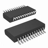
ISL59448IAZ-T7 Intersil, ISL59448IAZ-T7 Datasheet - Page 12

ISL59448IAZ-T7
Manufacturer Part Number
ISL59448IAZ-T7
Description
IC AMP MUX 2:1 500MHZ 24-QSOP
Manufacturer
Intersil
Datasheet
1.ISL59448IAZ-T7.pdf
(14 pages)
Specifications of ISL59448IAZ-T7
Applications
2:1 Multiplexer-Amplifier
Number Of Circuits
3
-3db Bandwidth
570MHz
Slew Rate
1600 V/µs
Current - Supply
31mA
Current - Output / Channel
180mA
Mounting Type
Surface Mount
Package / Case
24-QSOP
Lead Free Status / RoHS Status
Lead free / RoHS Compliant
Available stocks
Company
Part Number
Manufacturer
Quantity
Price
Company:
Part Number:
ISL59448IAZ-T7
Manufacturer:
Intersil
Quantity:
800
control signal rise and fall times less than 10ns the use of
termination resistors close to the part will minimize transients
coupled to the output.
Power-up Considerations
The ESD protection circuits use internal diodes from all pins
the V+ and V- supplies. In addition, a dV/dT- triggered clamp
is connected between the V+ and V- pins, as shown in the
Equivalent Circuits 1 through 4 section of the Pin Description
table. The dV/dT triggered clamp imposes a maximum
supply turn-on slew rate of 1V/µs. Damaging currents can
flow for power supply rates-of-rise in excess of 1V/µs, such
as during hot plugging. Under these conditions, additional
methods should be employed to ensure the rate of rise is not
exceeded.
Consideration must be given to the order in which power is
applied to the V+ and V- pins, as well as analog and logic
input pins. Schottky diodes (Motorola MBR0550T or
equivalent) connected from V+ to ground and V- to ground
(Figure 4) will shunt damaging currents away from the
internal V+ and V- ESD diodes in the event that the V+
supply is applied to the device before the V- supply.
If positive voltages are applied to the logic or analog video
input pins before V+ is applied, current will flow through the
internal ESD diodes to the V+ pin. The presence of large
decoupling capacitors and the loading effect of other circuits
connected to V+, can result in damaging currents through
the ESD diodes and other active circuits within the device.
Therefore, adequate current limiting on the digital and
analog inputs is needed to prevent damage during the time
the voltages on these inputs are more positive than V+.
HIZ State
An internal pull-down resistor ensures the device will be
active with no connection to the HIZ pin. The HIZ state is
established within approximately 15ns (Figure 14) by placing
a logic high (>2V) on the HIZ pin. If the HIZ state is selected,
the output impedance is ~1000Ω (Figure 6). The supply
current during this state is same as the active state.
V+ SUPPLY
V- SUPPLY
POWER
SIGNAL
LOGIC
GND
DE-COUPLING
CAPS
12
PROTECTION
SCHOTTKY
FIGURE 28. SCHOTTKY PROTECTION CIRCUIT
GND
S0
IN0
IN1
V+
V-
V+
V-
ISL59448
V+
V-
V+
V-
ENABLE and Power-down States
The enable pin is active low. An internal pull-down resistor
ensures the device will be active with no connection to the
ENABLE pin. The Power-down state is established within
approximately 200ns (Figure 22), if a logic high (>2V) is
placed on the ENABLE pin. In the power-down state, the
output has no leakage but has a large variable capacitance
(on the order of 15pF), and is capable of being back-driven.
Under this condition, large incoming slew rates can cause
fault currents of tens of mA. Therefore, the parallel
connection of multiple outputs is not recommended unless
the application can tolerate the limited powerdown output
impedance.
LE State
The ISL59448 is equipped with a Latch Enable pin. A logic
high (>2V) on the LE pin latches the last logic state. This
logic state is preserved when cycling HIZ or ENABLE
functions.
Limiting the Output Current
No output short circuit current limit exists on these parts. All
applications need to limit the output current to less than
50mA. Adequate thermal heat sinking of the parts is also
required.
CONTROL
LOGIC
V+
V-
OUT
EXTERNAL
CIRCUITS
March 29, 2006
FN6160.2


