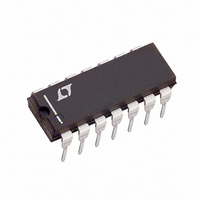
LT1256CN Linear Technology, LT1256CN Datasheet - Page 12

LT1256CN
Manufacturer Part Number
LT1256CN
Description
IC AMP VIDEO FADE CONTRLD 14-DIP
Manufacturer
Linear Technology
Datasheet
1.LT1256CSPBF.pdf
(24 pages)
Specifications of LT1256CN
Applications
Current Feedback
Number Of Circuits
1
-3db Bandwidth
40MHz
Slew Rate
300 V/µs
Current - Supply
14.5mA
Current - Output / Channel
40mA
Voltage - Supply, Single/dual (±)
5 V ~ 30 V, ±2.5 V ~ 15 V
Mounting Type
Through Hole
Package / Case
14-DIP (0.300", 7.62mm)
Lead Free Status / RoHS Status
Contains lead / RoHS non-compliant
Available stocks
Company
Part Number
Manufacturer
Quantity
Price
Part Number:
LT1256CN#PBF
Manufacturer:
LINEAR/凌特
Quantity:
20 000
APPLICATIONS
LT1251/LT1256
Signal Path Description
Figure 2 is the basic block diagram of the LT1251/LT1256
signal path with external resistors R
Both input stages are operating as noninverting amplifiers
with two input signals V
Each input stage has a unity-gain buffer from the nonin-
verting input to the inverting input. Therefore, the inverting
input is at the same voltage as the noninverting input. R
and R
buffers, approximately 27 .
K is a constant determined by the control circuit and can
be any value between 0 and 1. The control circuit is
described in a later section.
By inspection of the diagram:
12
I
1
2
R
represent the internal output resistances of these
1
R
R
V
G
G
1
1
1
R
R
U
F
F
1
1
1
INFORMATION
R
U
and V
F
R
R
1
G1
G2
R
2
V
V
I
I
1
2
.
1
1
2
V
O
R
R
R
W
R
14
G1
13
2
1
G
2
F
1
1
1
, R
R
R
–
+
+
–
F1
F2
F1
1
1
2
, R
Figure 2. Signal Path Block Diagram
G2
U
and R
I
I
1
2
F2
1 – K
1
K
.
Substituting and rearranging gives:
V
O
I
I
V
O
2
O
General Equation for the Noninverting Amplifier Case
I
1
O
R
KI
I
R
sR C
O
2
1
OL
R
OL
OL
1
R
R
1
R
V
G
G
1
R
2
sR C
2
2
K I
OL
C
R
OL
R
F
R
KV
R
R
2
1
G
F
G
F
1
2
1
1
2
R
+1
R
1
R
K
F
F
1
R
R
R
1
G
F
F
1
2
1
R
1251/56 BD
8
2
1
R
2
V
1
O
R
R
R
R
R
G
F
G
G
K V
F
V
2
2
2
2
2
O
2
R
R
R
1
F
1
F
2
2
2
K
R
R
G
F
2
2
1


