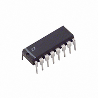
LT1204CN#PBF Linear Technology, LT1204CN#PBF Datasheet - Page 12

LT1204CN#PBF
Manufacturer Part Number
LT1204CN#PBF
Description
IC VIDEO MUX CFA 75MHZ 4IN 16DIP
Manufacturer
Linear Technology
Datasheet
1.LT1204CSWPBF.pdf
(20 pages)
Specifications of LT1204CN#PBF
Applications
4:1 Multiplexer-Amplifier
Number Of Circuits
1
-3db Bandwidth
75MHz
Slew Rate
1000 V/µs
Current - Supply
19mA
Current - Output / Channel
125mA
Voltage - Supply, Single/dual (±)
10 V ~ 30 V, ±5 V ~ 15 V
Mounting Type
Through Hole
Package / Case
16-DIP (0.300", 7.62mm)
Lead Free Status / RoHS Status
Lead free / RoHS Compliant
Available stocks
Company
Part Number
Manufacturer
Quantity
Price
LT1204
A
When the decoder turns off the tee switch (Q2 on) the
emitter base junctions of Q1 and Q3 become reverse-
biased while Q2 emitter absorbs current from I
do the reverse-biased emitter base junctions provide good
isolation, but any signal at V
further attenuated by the shunt impedance of Q2 emitter.
Current from I
Crosstalk performance is a strong function of the IC
package, the PC board layout as well as the IC design. The
die layout utilizes grounds between each input to isolate
adjacent channels, while the output and feedback pins are
on opposite sides of the die from the input. The layout of
a PC board that is capable of providing – 90dB all hostile
crosstalk at 10MHz is not trivial. That level corresponds to
a 30 V output below a 1V input at 10MHz. A demonstra-
tion board has been fabricated to show the component and
ground placement required to attain these crosstalk num-
12
PPLICATI
–100
–120
–20
–40
–60
–80
1
2
is routed to any on switch.
V
V
V
R
O
S
IN0
IN1,2,3
L
= 15V
= 100
= GND
All Hostile Crosstalk
U
= 0dBm
DEMO PCB #029
S
FREQUENCY (MHz)
I FOR ATIO
U
IN0
10
PDIP
coupling to Q1 emitter is
SO
DEMO PCB #028
W
1204 AI07
100
1
. Not only
U
bers. A graph of all hostile crosstalk for both the PDIP and
SO packages is shown. It has been found empirically from
these PC boards that capacitive coupling across the pack-
age of greater than 3fF (0.003pF) will diminish the rejec-
tion, and it is recommended that this proven layout be
copied into designs. The key to the success of the SO PC
board #028 is the use of a ground plane guard around Pin
13, the feedback pin.
PDIP PC Board #029, Component Side
VIN1
VIN2
VIN3
GND
VIN0
U1
R1
V–
C2
C4
+
DEMONSTRATION BOARD
R2
C1
+
R6
C3
LT1204 VIDEO MUX
V+
RF
(408) 432-1900
RO
VOUT
R3
ENABLE
S/D
REF
R1
R0
1204 AI09


