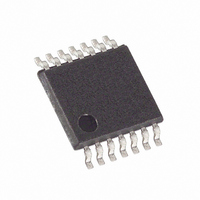
MAX4027EUD+ Maxim Integrated Products, MAX4027EUD+ Datasheet - Page 2

MAX4027EUD+
Manufacturer Part Number
MAX4027EUD+
Description
IC AMP VIDEO MUX 2CH 14-TSSOP
Manufacturer
Maxim Integrated Products
Datasheet
1.MAX4027EUD.pdf
(11 pages)
Specifications of MAX4027EUD+
Applications
2:1 Multiplexer-Amplifier
Number Of Circuits
3
-3db Bandwidth
225MHz
Slew Rate
1100 V/µs
Current - Supply
31mA
Current - Output / Channel
143mA
Voltage - Supply, Single/dual (±)
±4.5 V ~ 5.5 V
Mounting Type
Surface Mount
Package / Case
14-TSSOP
Lead Free Status / RoHS Status
Lead free / RoHS Compliant
ABSOLUTE MAXIMUM RATINGS
Positive Supply Voltage (V
Negative Supply Voltage (V
Amplifier Input Voltage (IN_ _) .........(V
Digital Input Voltage (EN, A/B) ...................-0.3V to (V
Output Short Circuit to GND (Note 1).........................Continuous
Output Short Circuit to V
225MHz, Triple, 2-Channel Video
Multiplexer-Amplifier
Stresses beyond those listed under “Absolute Maximum Ratings” may cause permanent damage to the device. These are stress ratings only, and functional
operation of the device at these or any other conditions beyond those indicated in the operational sections of the specifications is not implied. Exposure to
absolute maximum rating conditions for extended periods may affect device reliability.
DC ELECTRICAL CHARACTERISTICS
(V
2
Note 1: Continuous power-dissipation rating must also be observed.
Operating Supply Voltage Range
Positive Supply Current
Negative Supply Current
Input Voltage Range
Input Offset Voltage
Input Offset-Voltage Matching
Voltage Gain
Input Offset-Voltage Temperature
Coefficient
Input Bias Current
Input Resistance
DC Output Resistance
Disabled Output Resistance
DC Power-Supply Rejection Ratio
Output Voltage Swing
Output Short-Circuit Current
LOGIC CHARACTERISTICS (EN, A/B)
Logic-Low Threshold
Logic-High Threshold
Logic-Low Input Current
Logic-High Input Current
CC
_______________________________________________________________________________________
= 5V, V
PARAMETER
EE
= -5V, V
IN_ _
CC
CC
EE
or V
= 0V, R
to GND) ..................................+6V
to GND) ..................................-6V
EE
...........................................5s
L
SYMBOL
EE
= 150Ω to GND, T
R
TCV
V
V
PSRR
∆V
R
OUT(d)
V
V
V
OUT_
I
R
V
I
IN_ _
I
V
A
- 0.3V) to (V
OUT
I
CC
I
EE
I
SC
CC
EE
OS
IH
B
IL
IN
IH
IL
OS
V
OS
Inferred from the PSRR test
EN = GND
EN = 5V
EN = GND
EN = 5V
Inferred from voltage gain
T
T
Channel to channel
V
T
T
V
+1.25V
EN = 5V, V
V
V
V
A
A
A
A
OUT_
IN_ _
CC
IL
IH
= +25°C
= -40°C to +85°C
= +25°C
= -40°C to +85°C
= 0V
CC
CC
= +5.5V, V
= +4.5V to +5.5V, V
= -1.25V to
= ±2.5V
+ 0.3V)
+ 0.3V)
A
= -40°C to +85°C. Typical values are at T
OUT_
CC
CONDITIONS
= -2.5V to +2.5V (Note 3)
= +5.5V
Continuous Power Dissipation (T
Operating Temperature Range ...........................-40°C to +85°C
Storage Temperature Range .............................-65°C to +150°C
Junction Temperature .....................................................+150°C
Lead Temperature (soldering, 10s) .................................+300°C
14-Pin TSSOP (derate 9.1mW/°C above +70°C) .........727mW
14-Pin SO (derate 8.3mW/°C above +70°C)................667mW
EE
Channel on
Channel off
= -4.5V to -5.5V
±1.25
+4.5
±2.5
MIN
-4.5
100
A
1.9
2.0
60
1
= +25°C.) (Note 2)
A
= +70°C)
±1.75
±143
+5.0
±3.5
TYP
-5.0
400
350
2.0
1.6
±1
±1
±2
31
17
28
15
20
10
86
-4
1
MAX
+5.5
-5.5
±11
±12
±10
±18
600
-20
2.1
0.8
±6
39
24
36
21
UNITS
µV/°C
MΩ
mΩ
mA
mA
mV
mV
V/V
mA
dB
µA
kΩ
kΩ
µA
µA
V
V
V
V
V


