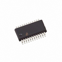
EL4501IU Intersil, EL4501IU Datasheet - Page 2

EL4501IU
Manufacturer Part Number
EL4501IU
Description
IC VIDEO FRONT END AMP 24-QSOP
Manufacturer
Intersil
Datasheet
1.EL4501IUZ.pdf
(19 pages)
Specifications of EL4501IU
Applications
Video Front End (VFE)
Number Of Circuits
1
-3db Bandwidth
100MHz
Slew Rate
96 V/µs
Current - Supply
10.5mA
Current - Output / Channel
70mA
Voltage - Supply, Single/dual (±)
4.5 V ~ 5.5 V
Mounting Type
Surface Mount
Package / Case
24-QSOP
Lead Free Status / RoHS Status
Contains lead / RoHS non-compliant
Available stocks
Company
Part Number
Manufacturer
Quantity
Price
Company:
Part Number:
EL4501IU
Manufacturer:
Intersil
Quantity:
120
Part Number:
EL4501IUZ
Manufacturer:
INTERSIL
Quantity:
20 000
Electrical Specifications
Absolute Maximum Ratings
Supply Voltage (V
Pin Voltage. . . . . . . . . . . . . . . . . . . . . . . . . . . .GND -0.3V, V
Storage Temperature Range . . . . . . . . . . . . . . . . . .-65°C to +150°C
Ambient Operating Temperature . . . . . . . . . . . . . . . .-40°C to +85°C
CAUTION: Stresses above those listed in “Absolute Maximum Ratings” may cause permanent damage to the device. This is a stress only rating and operation of the
device at these or any other conditions above those indicated in the operational sections of this specification is not implied.
IMPORTANT NOTE: All parameters having Min/Max specifications are guaranteed. Typ values are for information purposes only. Unless otherwise noted, all tests are
at the specified temperature and are pulsed tests, therefore: T
I
I
V
V
VIDEO AMPLIFIER SECTION
V
V
+I
-I
dG
dP
BW
BW1
SR
V
t
R
C
A
DC-RESTORE SECTION
CMIR
V
TCV
I
SA
SD
S
B
PARAMETER
OUT
VOL
S
SD
OP
ON
RL
OS
IN
IN
OUT
OS
S
Input Supply Current
Digital Supply Current
Input Supply Voltage Range
Digital Input Supply Voltage Range
Positive Output Voltage Swing (VIDEO OUT)
(Note 1)
Negative Output Voltage Swing (VIDEO OUT)
(Note 1)
Positive Output Current (VIDEO OUT)
Negative Output Current (VIDEO OUT)
Differential Gain Error (VIDEO OUT) (Note 2) A
Differential Phase Error (VIDEO OUT)
(Note 2)
Bandwidth
Bandwidth
Slew Rate
Ref Level Range
Settling Time
Input Resistance (VIDEO IN)
Input Capacitance (VIDEO IN)
Open Loop Voltage Gain
Common Mode Input Range (REF IN)
Input Offset Voltage
Input Offset Voltage Temperature Coefficient
Input Bias Current (REF IN)
to GND) . . . . . . . . . . . . . . . . . . . . . . . . . . . .+6V
DESCRIPTION
2
V
S
(T
= V
A
= 25°C)
SD
= 5V, GND = 0V, T
J
= T
C
S
= T
+0.3V
A
A
No load
No load, V
R
R
-3dB, G = 1, R
±0.1dB, G = 2, R
R
R
R
R
R
R
R
A
-3dB, G = 1, R
25% to 75%, 3.5V
to 0.1%, V
R
DC restored
V
= 25°C, Input Video = 1V
V
V
L
L
L
L
L
L
L
L
L
L
CM
EL4501
= 150Ω to V
= 150Ω to GND
= 1kΩ to V
= 150Ω to V
= 150Ω to GND
= 1kΩ to V
= 1, R
= 1, R
= 10Ω to V
= 10Ω to V
= no load, V
= 150Ω to GND, V
= 0V to 3.5V
L
L
IN
IN
= 10kΩ, R
= 10kΩ, R
Operating Junction Temperature . . . . . . . . . . . . . . . . . . . . . . . 125°C
Power Dissipation . . . . . . . . . . . . . . . . . . . . . . . . . . . . . See Curves
Maximum Continuous Current (VIDEO OUT) . . . . . . . . . . . . . 50mA
= 0V
= 0V to 3V
S
S
S
S
L
L
CONDITIONS
/2
/2
S
S
OUT
/2
/2
= 10kΩ to GND, R
= 150Ω to GND, R
/2
/2
L
P-P
= 150Ω to GND
= 0.5V to 3V
F
F
, R
OUT
= 0Ω
= 0Ω
L
= 150Ω, R
P-P
= 0.5V to 3V
, R
FREQ
F
F
F
= 0
= 0
= 0
= 130kΩ
4.65
4.20
4.85
MIN
-50
-10
7.5
1.9
4.5
4.5
60
80
0.001
0/3.5
0/3.5
TYP
10.5
4.70
4.60
4.90
0.15
0.06
0.05
0.05
0.03
100
115
±20
2.3
-60
1.5
70
60
96
35
65
50
10
8
MAX
13.5
0.30
0.25
0.20
5.5
5.5
10
4
µV/°C
UNIT
MHz
MHz
MHz
V/µs
mA
mA
mA
mA
mV
kΩ
dB
dB
µA
pF
ns
%
V
V
V
V
V
V
V
V
V
V
°


