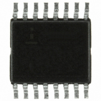
ISL59830AIAZ Intersil, ISL59830AIAZ Datasheet - Page 13

ISL59830AIAZ
Manufacturer Part Number
ISL59830AIAZ
Description
IC VIDEO DRIVER TRUE SGL 16-QSOP
Manufacturer
Intersil
Datasheet
1.ISL59830AIAZ.pdf
(15 pages)
Specifications of ISL59830AIAZ
Applications
Driver
Output Type
Rail-to-Rail
Number Of Circuits
3
-3db Bandwidth
200MHz
Slew Rate
500 V/µs
Current - Supply
120mA
Current - Output / Channel
50mA
Voltage - Supply, Single/dual (±)
3 V ~ 3.6 V
Mounting Type
Surface Mount
Package / Case
16-QSOP
Lead Free Status / RoHS Status
Lead free / RoHS Compliant
Available stocks
Company
Part Number
Manufacturer
Quantity
Price
Part Number:
ISL59830AIAZ
Manufacturer:
INTERSIL
Quantity:
20 000
standard encodes sync on the Y channel and it is a negative-
going signal; easily handled by the ISL59830A without the need
of an additional supply as the ISL59830A generates a negative
rail placed at negative 1/2 the positive supply. Additionally, the
Pb and Pr are bipolar analog signals and the video signals are
negative-going; and again easily handled by the ISL59830A.
Driving Capacitive Loads and Cables
The ISL59830A, internally-compensated to drive 75Ω cables,
will drive 10pF loads in parallel with 1kΩ with less than 5dB of
peaking. If less peaking is required, a small series resistor,
usually between 5Ω to 50Ω, can be placed in series with the
output. This will reduce peaking at the expense of a slight
closed loop gain reduction. When used as a cable driver,
double termination is always recommended for reflection-free
performance. For those applications, a back-termination series
resistor at the amplifier's output will isolate the amplifier from
the cable and allow extensive capacitive drive. However, other
applications may have high capacitive loads without a back-
termination resistor. Again, a small series resistor at the output
can help to reduce peaking. The ISL59830A is a triple amplifier
designed to drive three channels; simply deal with each
channel separately as described in this section.
DC-Restore
When the ISL59830A is AC-coupled it becomes necessary
to restore the DC reference for the signal. This is
accomplished with a DC-restore system applied between the
capacitive "AC" coupling and the input of the device. Refer to
Application Circuit for reference DC-restore solution.
Disable/Power-Down
The ISL59830A can be disabled and its output placed in a
high impedance state. The turn-off time is around 25ns and
the turn-on time is around 200ns. When disabled, the
amplifier's supply current is reduced to 0.9mA typically,
thereby effectively eliminating the power consumption. The
amplifier's power-down can be controlled by standard TTL or
CMOS signal levels at the EN and PD pins. The applied
logic signal is relative to V
float or applying a signal that is less than 0.8V above V
enable the amplifier. The amplifier will be disabled when the
signal at EN pin is 2V above V
disabled (EN pin is high) whenever the charge pump is
disabled (PD pin is high). EN and PD pins should be
connected together to allow amplifier and charge pump
to enable/disable simultaneously.
Output Drive Capability
The ISL59830A does not have internal short-circuit
protection circuitry. A short-circuit current of 80mA sourcing
and 150mA sinking for the output is connected to half way
between the rails with a 10Ω resistor. If the output is shorted
indefinitely, the power dissipation could easily increase such
that the part will be destroyed. Maximum reliability is
maintained if the output current never exceeds ±40mA, after
which the electro-migration limit of the process will be
S
- pin. Letting the EN and PD pins
13
S
-. The amplifier must be
S
- will
ISL59830A
exceeded and the part will be damaged. This limit is set by
the design of the internal metal interconnections.
Power Dissipation
With the high output drive capability of the ISL59830A, it is
possible to exceed the +150°C absolute maximum junction
temperature under certain load current conditions.
Therefore, it is important to calculate the maximum junction
temperature for an application to determine if load conditions
or package types need to be modified to assure operation of
the amplifier in a safe operating area.
The maximum power dissipation allowed in a package is
determined according to:
PD
Where:
The maximum power dissipation actually produced by an IC
is the total quiescent supply current times the total power
supply voltage, plus the power in the IC due to the load, or:
for sourcing:
for sinking:
Where:
By setting the two P
can solve the output current and R
overheat.
PD
PD
T
T
Θ
V
I
V
R
I
i = Number of output channels
MAX
SMAX
LOAD
MAX
MAX
AMAX
JMAX
S
OUT
LOAD
JA
= Supply voltage
= Thermal resistance of the package
=
=
=
= Maximum output voltage of the application
= Load current
= Maximum quiescent supply current
= Maximum junction temperature
= Maximum ambient temperature
= Load resistance tied to ground
T
-------------------------------------------- -
V
V
JMAX
S
S
×
×
I
I
Θ
SMAX
SMAX
–
JA
T
DMAX
AMAX
+
+
(
(
V
V
S
OUT
equations equal to each other, we
–
V
i V
OUT
–
S
i
LOAD
)
)
×
×
V
-----------------
I
LOAD
OUT
R
to avoid the device
L
i
i
i
September 26, 2006
FN6233.3


