LM6588MA/NOPB National Semiconductor, LM6588MA/NOPB Datasheet - Page 10
LM6588MA/NOPB
Manufacturer Part Number
LM6588MA/NOPB
Description
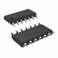
IC OPAMP TFT-LCD QUAD 16V 14SOIC
Manufacturer
National Semiconductor
Series
VIP10™r
Datasheet
1.LM6588MANOPB.pdf
(16 pages)
Specifications of LM6588MA/NOPB
Applications
TFT-LCD Panels: Gamma Buffer, VCOM Driver
Output Type
Rail-to-Rail
Number Of Circuits
4
-3db Bandwidth
24MHz
Slew Rate
15 V/µs
Current - Supply
800µA
Current - Output / Channel
230mA
Voltage - Supply, Single/dual (±)
5 V ~ 16 V, ±2.5 V ~ 8 V
Mounting Type
Surface Mount
Package / Case
14-SOIC (0.154", 3.90mm Width)
Number Of Channels
4
Voltage Gain Db
106 dB
Common Mode Rejection Ratio (min)
70 dB
Input Offset Voltage
4 mV at 5 V
Operating Supply Voltage
9 V, 12 V, 15 V
Supply Current
4 mA at 5 V
Maximum Operating Temperature
+ 85 C
Maximum Dual Supply Voltage
+/- 8 V
Minimum Operating Temperature
- 40 C
Lead Free Status / RoHS Status
Lead free / RoHS Compliant
Other names
*LM6588MA
*LM6588MA/NOPB
LM6588MA
*LM6588MA/NOPB
LM6588MA


www.national.com
Application Notes
ground is a uniform low impedance. If a four layer board
cannot be used, consider pouring a plane on one side of a
two layer board. If this cannot be done be sure to use as
wide a trace as practicable and use extra decoupling capaci-
tors to minimize the AC variations on the ground rail.
Decoupling
A high-speed, high-current amp like the LM6588 must have
generous decoupling capacitors. They should be as close to
the power pins as possible. Putting them on the back side
opposite the power pins may give the tightest layout. If
ground and power planes are available, the placement of the
decoupling caps are not as critical.
Breadboards
The high currents and high frequencies the LM6588 oper-
ates at, as well as thermal considerations, require that pro-
totyping of the design be done on a circuit board as opposed
to a “Proto-Board” style breadboard.
STABILITY
General:
High speed parts with large output current capability require
special care to insure lack of oscillations. Keep the ”+” pin
isolated from the output to insure stability. As noted above
care should be take to insure the large output currents do not
appear in the ground or ground plane and then get coupled
into the “+” pin. As always, good tight layout is essential as is
adequate use of decoupling capacitors on the power sup-
plies.
Unity Gain
The unity gain or voltage-follower configuration is the most
subject to oscillation. If a part is stable at unity gain it is
almost certain to work in other configurations. In certain
applications where the part is setting a reference voltage or
is being used as a buffer greater stability can be achieved by
configuring the part as a gain of −1 or −2 or +2.
Phase Margin
The phase margin of an op amps gain-phase plot is an
indication of the stability of the amp. It is desirable to have at
least 45˚C of phase margin to insure stability in all cases.
The LM6588 has 60˚C of phase margin even with it’s large
output currents and Rail-to-Rail output stage, which are
generally more prone to stability issues.
Capacitive Load
The LM6588 can withstand 30pF of capacitive load in a unity
gain configuration before stability issues arise. At very large
capacitances, the load capacitor will attenuate the gain like
any other heavy load and the part becomes stable again.
The LM6588 will be stable at 330nF and higher load capaci-
tance. Refer to the chart in the Typical Performance Char-
acteristics section.
OUTPUT
Swing vs. Current
The LM6588 will get to about 25mV or 30mV of either rail
when there is no load. The LM6588 can sink or source
hundreds of milliamperes while remaining less then 0.5V
away from the rail. It should be noted that if the outputs are
(Continued)
10
driven to the rail and the part can no longer maintain the
feedback loop, the internal circuitry will deliver large base
currents into the huge output transistors, trying to get the
outputs to get past the saturation voltage. The base currents
will approach 16 milliamperes and this will appear as an
increase in power supply current. Operating at this power
dissipation level for extended periods will damage the part,
especially in the higher thermal resistance TSSOP package.
Because of this phenomenon, unused parts should not have
the inputs strapped to either rail, but should have the inputs
biased at the midpoint or at least a diode drop (0.6V) within
the rails.
Self Heating
As discussed above the LM6588 is capable of significant
power by virtue of its 200mA current handling capability. A
TSSOP package cannot sustain these power levels for more
then a brief period.
TFT Display Application
INTRODUCTION
In today’s high-resolution TFT displays, op amps are used
for the following three functions:
1. V
2. Gamma Buffer
3. Panel Repair Buffer
All of these functions utilize op amps as non-inverting, unity-
gain buffers. The V
that supply a well regulated DC voltage. A Panel Repair
Buffer, on the other hand, provides a high frequency signal
that contains part of the display’s visual image.
In an effort to reduce production costs, display manufactur-
ers use a minimum variety of different parts in their TFT
displays. As a result, the same type of op amp will be used
for the V
To perform all these functions, such an op amp must have
the following characteristics:
1. Large output current drive
2.
3. Rail to rail output swing
4. Medium speed gain bandwidth and slew rate
The LM6588 meets these requirements. It has a rail-to-rail
input and output, typical gain bandwidth and slew rate of
15MHz and 15V/µs, and it can supply up to 200mA of output
current. The following sections will describe the operation of
V
showing how the LM6588 is well suited for each of these
functions.
BRIEF OVERVIEW OF TFT DISPLAY
To better understand these op amp applications, let’s first
review a few basic concepts of how a TFT display operates.
Figure 1 is a simplified illustration of an LCD pixel. The top
and bottom plates of each pixel consist of Indium-Tin oxide
(ITO), which is a transparent, electrically conductive mate-
rial. ITO lies on the inner surfaces of two glass substrates
that are the front and back glass panels of a TFT display.
Sandwiched between the two ITO plates is an insulating
material (liquid crystal) that alters the polarization of light to a
lesser a greater amount, depending on how much voltage
(V
placed on the outer surfaces of the two glass substrates,
which in combination with the liquid crystal create a variable
COM
PIXEL
Rail to rail input common mode range
COM
Drivers, Gamma Buffers, and Panel Repair Buffers,
) is applied across the two plates. Polarizers are
COM
Driver
Driver, Gamma Buffer, and Panel Repair Buffer.
COM
Driver and Gamma Buffer are buffers
Related parts for LM6588MA/NOPB
Image
Part Number
Description
Manufacturer
Datasheet
Request
R

Part Number:
Description:
Op Amps
Manufacturer:
National Semiconductor
Datasheet:
Part Number:
Description:
National Semiconductor [8-Bit D/A Converter]
Manufacturer:
National Semiconductor
Datasheet:
Part Number:
Description:
National Semiconductor [Media Coprocessor]
Manufacturer:
National Semiconductor
Datasheet:
Part Number:
Description:
Digitally Controlled Tone and Volume Circuit with Stereo Audio Power Amplifier, Microphone Preamp Stage and National 3D Sound
Manufacturer:
National Semiconductor
Datasheet:
Part Number:
Description:
Digitally Controlled Tone and Volume Circuit with Stereo Audio Power Amplifier, Microphone Preamp Stage and National 3D Sound
Manufacturer:
National Semiconductor
Datasheet:
Part Number:
Description:
AC97 Rev 2 Codec with Sample Rate Conversion and National 3D Sound
Manufacturer:
National Semiconductor
Part Number:
Description:
Manufacturer:
National Semiconductor
Datasheet:
Part Number:
Description:
Manufacturer:
National Semiconductor
Datasheet:
Part Number:
Description:
General Purpose, Low Voltage, Low Power, Rail-to-Rail Output Operational Amplifiers
Manufacturer:
National Semiconductor
Datasheet:
Part Number:
Description:
8-bit 20 MSPS flash A/D converter.
Manufacturer:
National Semiconductor
Datasheet:
Part Number:
Description:
Low Noise Quad Operational Amplifier
Manufacturer:
National Semiconductor
Datasheet:
Part Number:
Description:
Quad Differential Line Receivers
Manufacturer:
National Semiconductor
Datasheet:
Part Number:
Description:
Quad High Speed Trapezoidal? Bus Transceiver
Manufacturer:
National Semiconductor
Datasheet:
Part Number:
Description:
Dual Line Receiver
Manufacturer:
National Semiconductor
Datasheet: