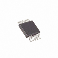
MAX4374TEUB Maxim Integrated Products, MAX4374TEUB Datasheet - Page 2

MAX4374TEUB
Manufacturer Part Number
MAX4374TEUB
Description
IC AMP GAIN +20V/V PREC 10-UMAX
Manufacturer
Maxim Integrated Products
Type
Amplifier, Comparator, Referencer
Datasheet
1.MAX4374HESD.pdf
(13 pages)
Specifications of MAX4374TEUB
Applications
Current Sensing, Power Management
Mounting Type
Surface Mount
Package / Case
10-MSOP, Micro10™, 10-uMAX, 10-uSOP
Lead Free Status / RoHS Status
Contains lead / RoHS non-compliant
Available stocks
Company
Part Number
Manufacturer
Quantity
Price
Part Number:
MAX4374TEUB
Manufacturer:
MAXIM/美信
Quantity:
20 000
Company:
Part Number:
MAX4374TEUB+T
Manufacturer:
MAXIM
Quantity:
209
Part Number:
MAX4374TEUB+T
Manufacturer:
MAXIM/美信
Quantity:
20 000
ABSOLUTE MAXIMUM RATINGS
V
OUT to GND ................................................-0.3V to the lesser of
CIN1, CIN2, RESET to GND ........................-0.3V to the lesser of
Differential Input Voltage (V
COUT1, COUT2 to GND........................................-0.3V to +6.0V
Current into Any Pin..........................................................±10mA
Low-Cost, Micropower, High-Side Current-Sense
Amplifier + Comparator + Reference ICs
ELECTRICAL CHARACTERISTICS
(V
Typical values are at T
Stresses beyond those listed under “Absolute Maximum Ratings” may cause permanent damage to the device. These are stress ratings only, and functional
operation of the device at these or any other conditions beyond those indicated in the operational sections of the specifications is not implied. Exposure to
absolute maximum rating conditions for extended periods may affect device reliability.
2
Operating Voltage Range
(Note 2)
Common-Mode Input Range
(Note 3)
Common-Mode Rejection
CC
Supply Current
Leakage Current
Input Bias Current
Full-Scale Sense Voltage
(Note 4)
Input Offset Voltage
Total OUT Voltage Error
(Note 5)
OUT Voltage Low
OUT Voltage High
CC
, RS+, RS- to GND ...........................................-0.3V to +30V
_______________________________________________________________________________________
= +2.7V to +28V, V
PARAMETER
A
= +25°C.) (Note 1)
RS+
RS
+ - V
= 0 to +28V, V
RS
SYMBOL
I
RS+,
V
-) ..............................±0.3V
V
CMR
V
V
V
SENSE
I
V
V
V
I
I
CMR
RS+
OUT
OUT
CC -
RS-
CC
CC
OS
OH
I
RS-
(V
(V
CC
CC
SENSE
V
V
V
V
V
V
V
V
(Note 11)
Gain = +20V/V, +50V/V, V
Gain = +100V/V, V
V
100mV
(Note 6)
V
V
V
V
V
+ 0.3V) or +15V
+ 0.3V) or +12V
RS+
RS+
CC
RS+
RS+
RS+
RS+
CC
SENSE
SENSE
RS+
CC
RS+
CC
= 0V, V
= V
= 2.7V,
= 2.7V, I
= 0V, V
> 2V
> 2V, V
> 2V
≤ 2V
> 2V
≤ 2V
= 12V
= 12V (Note 7)
RS+
=
= 6.25mV, V
RS+
= 12V
SENSE
RESET
OUT
V
V
V
V
V
CONDITIONS
= 28V
CC
RS+
CC
RS+
CC
= -500µA, V
RS+
= 5mV
= 0V, R
= 12V,
= 28V,
= 12V, V
CC
= 12V
= 28V
Continuous Power Dissipation (T
Operating Temperature Range ...........................-40°C to +85°C
Junction Temperature ......................................................+150°C
Storage Temperature Range .............................-65°C to +150°C
Lead Temperature (soldering, 10s) .................................+300°C
Soldering Temperature (reflow) .......................................+260°C
= 12V
= 12V,
T
T
I
I
8-Pin µMAX (derate 4.1mW/°C above +70°C) .............330mW
8-Pin SO (derate 5.9mW/°C above +70°C)..................471mW
10-Pin µMAX (derate 5.6mW/°C above +70°C) ...........444mW
14-Pin SO (derate 8.3mW/°C above +70°C)................667mW
OUT
OUT
A
A
RS+
RS+
LOAD
= +25°C
= T
T
T
T
T
= 10µA
= 100µA
A
A
A
A
RS+
MIN
= 12V
= 0.1V
= +25°C
= T
= +25°C
= T
= 1MΩ, T
to T
= 12V
MIN
MIN
MAX
to T
to T
MAX
MAX
A
= T
MIN
MIN
150
100
2.7
-25
-50
0
0
0
to T
A
MAX
= +70°C)
±0.015
±0.30
±0.35
±5.0
±5.0
TYP
170
120
, unless otherwise noted.
0.1
2.5
8.5
85
50
MAX
±0.5
0.25
100
2.5
2.0
±2
±3
±2
±3
28
28
65
4
4
1
2
UNITS
mV
mV
mV
dB
µA
µA
µA
%
V
V
V


