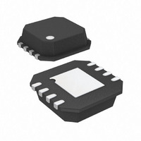
AD8337BCPZ-WP Analog Devices Inc, AD8337BCPZ-WP Datasheet - Page 9

AD8337BCPZ-WP
Manufacturer Part Number
AD8337BCPZ-WP
Description
IC AMP VGA DC-COUPLED GP 8-LFCSP
Manufacturer
Analog Devices Inc
Series
X-AMP®r
Type
Variable Gain Amplifierr
Datasheet
1.AD8337BCPZ-WP.pdf
(32 pages)
Specifications of AD8337BCPZ-WP
Applications
Signal Processing
Mounting Type
Surface Mount
Package / Case
8-LFCSP
For Use With
AD8337-EVALZ-SS - BOARD EVALUATION FOR AD8337 SSAD8337-EVALZ-INV - BOARD EVALUATION FOR AD8337 INSAD8337-EVALZ - BOARD EVALUATION FOR AD8337
Lead Free Status / RoHS Status
Lead free / RoHS Compliant
Available stocks
Company
Part Number
Manufacturer
Quantity
Price
Company:
Part Number:
AD8337BCPZ-WP
Manufacturer:
STM
Quantity:
2 483
Figure 16. Output Offset Voltage Histogram for Three Values of V
–10
80
70
40
100
60
50
30
20
10
0.1
10
–2
–4
–6
–8
1k
10
0
Figure 15. Offset Voltage vs. V
–800
8
6
4
2
0
1
1M
–15
500 UNITS
Figure 17. VGA Output Impedance vs. Frequency
V
V
V
+85°C
+25°C
–40°C
V
V
GAIN
GAIN
GAIN
–600
S
S
= ±2.5V
= ±5V
–10
= –0.4V
= 0V
= +0.4V
–400
OUTPUT OFFSET VOLTAGE (mV)
–5
V
S
= ±2.5V
(See Figure 48)
(See Figure 49)
–200
10M
FREQUENCY (Hz)
0
V
GAIN
5
GAIN
0
(mV)
at Three Temperatures
10
200
V
S
15
100M
= ±5V
400
20
600
25
500M
800
GAIN
Rev. C | Page 9 of 32
Figure 20. Short-Circuit, Input-Referred Noise vs. Frequency at Maximum
Figure 19. Short-Circuit, Input-Referred Noise at Three Temperatures
Figure 18. Output-Referred Noise vs. V
Gain—Inverting and Noninverting Preamp Gain = −1 and +2
40
35
30
25
20
15
25
20
15
10
–800
–800
100k
5
0
7
6
5
4
3
2
1
0
V
R
GAIN
FB1
+85°C
+25°C
–40°C
–600
–600
= R
= 0.7V
FB2
–400
–400
= 100Ω
1M
(See Figure 50)
(See Figure 50)
(See Figure 50)
–200
–200
PREAMP GAIN = –1
PREAMP GAIN = +2
FREQUENCY (Hz)
V
V
GAIN
GAIN
0
0
(mV)
(mV)
GAIN
200
200
at Three Temperatures
10M
400
400
600
600
AD8337
+85°C
+25°C
–40°C
100M
800
800


