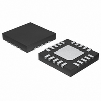
MAX9726AETP+T Maxim Integrated Products, MAX9726AETP+T Datasheet - Page 2

MAX9726AETP+T
Manufacturer Part Number
MAX9726AETP+T
Description
IC AMP AUDIO .124W STER 20TQFN
Manufacturer
Maxim Integrated Products
Series
DirectDrive™r
Type
Class ABr
Datasheet
1.MAX9726BETP.pdf
(24 pages)
Specifications of MAX9726AETP+T
Output Type
Headphones, 2-Channel (Stereo)
Max Output Power X Channels @ Load
124mW x 2 @ 16 Ohm
Voltage - Supply
2.7 V ~ 5.5 V
Features
Bass Boost, Depop, I²C, Mute, Short-Circuit and Thermal Protection, Shutdown, Volume Control
Mounting Type
Surface Mount
Package / Case
20-TQFN Exposed Pad
Lead Free Status / RoHS Status
Lead free / RoHS Compliant
ABSOLUTE MAXIMUM RATINGS
V
PV
SGND to PGND .....................................................-0.3V to +0.3V
C1P to PGND..............................................-0.3V to (V
C1N to PGND............................................(PV
PV
IN_ to SGND...................................(SV
FB_ to SGND..................................(SV
SDA, SCL to PGND ....................................-0.3V to (V
SHDN to PGND ..........................................-0.3V to (V
OUT_ to SGND ............................................................-3V to +3V
BM_ to SGND ..............................................................-3V to +3V
Duration of OUT_ Short Circuit to PGND....................Continuous
DirectDrive, Headphone Amplifier with
BassMax, I
ELECTRICAL CHARACTERISTICS (5V Supply)
(V
ume (overall gain = 0dB), BassMax disabled. Load connected between OUT_ and PGND where specified. T
otherwise noted. Typical values are at T
Stresses beyond those listed under “Absolute Maximum Ratings” may cause permanent damage to the device. These are stress ratings only, and functional
operation of the device at these or any other conditions beyond those indicated in the operational sections of the specifications is not implied. Exposure to
absolute maximum rating conditions for extended periods may affect device reliability.
2
GENERAL
Supply Voltage Range
Quiescent Supply Current
Shutdown Supply Current
Turn-On Time
Turn-Off Time
Thermal-Shutdown Threshold
Thermal-Shutdown Hysteresis
HEADPHONE AMPLIFIER
Output Offset Voltage
Input Offset Voltage of Input
Amplifier
Input Bias Current
BMR, BML Input Bias Current
Power-Supply Rejection Ratio
(Note 2)
Output Power
Total Harmonic Distortion Plus
Noise
DD
DD
SS
SS
_ _ _ _ _ _ _ _ _ _ _ _ _ _ _ _ _ _ _ _ _ _ _ _ _ _ _ _ _ _ _ _ _ _ _ _ _ _ _ _ _ _ _ _ _ _ _ _ _ _ _ _ _ _ _ _ _ _ _ _ _ _ _ _ _ _ _ _ _ _ _ _ _ _ _ _ _ _ _ _ _ _ _ _ _ _ _ _ _ _ _ _ _ _ _ _ _ _ _ _ _ _ _ _ _ _ _ _ _ _ _ _ _ _ _ _ _ _ _ _ _ _ _ _ _ _ _ _ _ _ _ _ _ _ _ _ _ _ _ _ _ _ _ _ _ _ _ _ _ _ _ _ _ _ _ _ _ _ _ _ _ _ _ _ _ _ _ _ _ _ _ _ _ _
to PGND............................................................-0.3V to +6V
, SV
to SV
= SHDN = 5V, PGND = SGND = 0V, C1 = C2 = 1µF, C
SS
SS
PARAMETER
to PGND ................................................+0.3V to -6V
.........................................................-0.3V to +0.3V
2
C, Volume and Gain Control
SYMBOL
I
SS
SS
DD_SHDN
I
THD+N
T
BIAS_BB
V
A
T
PSRR
P
THRES
V
t
V
OSHP
- 0.3V) to (V
- 0.3V) to (V
t
HYST
I
OFF
OUT
DD
ON
= +25°C.) (Note 1)
I
DD
OS
B
SS
- 0.3V) to +0.3V
No load
SHDN
Measured between OUT_ and SGND, gain
= 0dB, R
(Note 2)
Referenced to SGND, measured between
FBR, FBL, and SGND
DC, V
f = 1kHz, 100mV
f = 20kHz, 100mV
THD+N = 1%,
f
R
R
IN
L
L
DD
DD
DD
DD
DD
= 1kHz
= 16Ω, P
= 32Ω, P
+ 0.3V)
+ 0.3V)
+ 0.3V)
+ 0.3V)
+ 0.3V)
DD
= 0V
IN
= 2.7V to 5.5V
PREG
= R
OUT
OUT
CONDITIONS
F
= C
R
R
P-P
= 15mW, f
= 30mW, f
= 10kΩ, T
L
L
P-P
Continuous Current Into/Out of:
Continuous Power Dissipation (T
Operating Temperature Range ...........................-40°C to +85°C
Junction Temperature ......................................................+150°C
Storage Temperature Range .............................-65°C to +150°C
OUTL and OUTR ESD Protection (Human Body Model)....±7.5kV
Bump Temperature (soldering) Reflow............................+230°C
Lead Temperature (soldering, 10s) .................................+300°C
= 16Ω
= 32Ω
NREG
ripple
V
Any Other Pin................................................................±20mA
20-Bump UCSP (derate 10mW/°C above +70°C) .......800mW
20-Pin TQFN (derate 25.6mW/°C above +70°C) .......2051mW
ripple
DD
, C1P, PGND, C1N, PV
= 1µF, BM_ = 0V, R
A
IN
IN
= +25°C
= 1kHz
= 1kHz
IN
MIN
2.7
80
= 10kΩ, R
SS
, SV
A
= +70°C, multilayer board)
SS
+150
±0.6
TYP
0.04
0.02
±20
±20
440
124
104
5.5
, or OUT_ ...........±850mA
12
97
85
74
8
1
3
A
F
= T
= 10kΩ, maximum vol-
MIN
±100
±100
MAX
5.5
10
15
10
to T
MAX
UNITS
, unless
mW
mA
mV
mV
dB
µA
°C
°C
nA
nA
µs
µs
%
V


