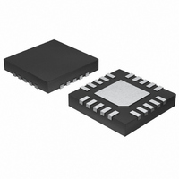
MAX9726BETP+T Maxim Integrated Products, MAX9726BETP+T Datasheet - Page 20

MAX9726BETP+T
Manufacturer Part Number
MAX9726BETP+T
Description
IC AMP AUDIO .124W STER 20TQFN
Manufacturer
Maxim Integrated Products
Series
DirectDrive™r
Type
Class ABr
Datasheet
1.MAX9726BETP.pdf
(24 pages)
Specifications of MAX9726BETP+T
Output Type
Headphones, 2-Channel (Stereo)
Max Output Power X Channels @ Load
124mW x 2 @ 16 Ohm
Voltage - Supply
2.7 V ~ 5.5 V
Features
Bass Boost, Depop, I²C, Mute, Short-Circuit and Thermal Protection, Shutdown, Volume Control
Mounting Type
Surface Mount
Package / Case
20-TQFN Exposed Pad
Lead Free Status / RoHS Status
Lead free / RoHS Compliant
Figure 10 shows the MAX9726 configured as a sum-
ming amplifier, which allows multiple audio sources to
be linearly mixed together. Using this configuration, the
output of the MAX9726 is equal to the weighted sum of
the input signals:
As shown in the above equation, the weighting or
amount of gain applied to each input signal source is
determined by the ratio of R
resistor (R
source. When BassMax is enabled, the low-frequency
gain (A
Setting Components section) adds to the gain deter-
mined by R
dynamic range of the MAX9726 is not exceeded when
BassMax is enabled and/or when the input signals are
at their maximum values and in phase with each other.
DirectDrive, Headphone Amplifier with
BassMax, I
Figure 10. Summing Amplifier
20
V
IN1
V
IN2
V
______________________________________________________________________________________
IN3
DIAGRAM SHOWN WITH BassMax DISABLED.
V
OUT
BOOST
C
IN1
IN
F
_
C
C
Summing Amplifier (Audio Mixer)
and R
IN
=
IN
, R
) set by R1, R2, and C3 (see the Gain-
−
R
⎛
⎜
⎝
IN1
IN2
V
R
R
IN
IN2
IN_
IN3
1
, R
R
. Select R
R
IN
IN3
F
1
IN_
+
) connected to each signal
2
V
V
FB_
F
IN
C, Volume and Gain Control
=
and the respective input
2
-(
F
MAX9726
V
R
IN1
and R
R
R
IN
F
F
R
R
2
IN1
F
+
+
IN_
FB_
V
V
IN2
IN
R
3
such that the
R
IN2
F
R
R
+
IN
F
TO
ATTENUATOR
STAGE
V
IN3
3
⎞
⎟
⎠
R
R
IN3
F
)
Proper layout and grounding are essential for optimum
performance. Connect PGND and SGND together at a
single point (star ground point) on the PC board.
Connect PV
connection with a 1µF capacitor to PGND. Bypass V
PREG, and NREG to PGND with a 1µF capacitor. Place
the power-supply bypass capacitor and the charge-
pump hold capacitor as close as possible to the
MAX9726. Route PGND, and all traces that carry
switching transients, away from SGND and the audio
signal path. Route digital signal traces away from the
audio signal path. Make traces perpendicular to each
other when routing digital signals over or under audio
signals.
The TQFN package features an exposed pad that
improves thermal efficiency. Ensure that the exposed
pad is electrically isolated from PGND, SGND, and
V
board layout dictates that the exposed pad cannot
be left unconnected.
For the latest application details on UCSP construction,
dimensions, tape carrier information, PC board tech-
niques, bump-pad layout, and recommended reflow
temperature profile, as well as the latest information on
reliability testing results, go to Maxim’s website at
www.maxim-ic.com/ucsp and look up the Application
Note: UCSP—A Wafer-Level Chip-Scale Package .
DD
. Connect the exposed pad to PV
UCSP Applications Information
SS
to SV
SS
at the device and bypass this
Layout and Grounding
SS
when the
DD
,


