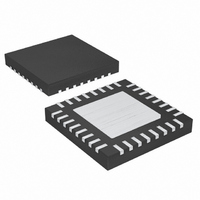
MAX9766ETJ+ Maxim Integrated Products, MAX9766ETJ+ Datasheet - Page 20

MAX9766ETJ+
Manufacturer Part Number
MAX9766ETJ+
Description
IC AMP AUDIO .75W MONO AB 32TQFN
Manufacturer
Maxim Integrated Products
Type
Class ABr
Datasheet
1.MAX9766ETJ.pdf
(33 pages)
Specifications of MAX9766ETJ+
Output Type
1-Channel (Mono) with Stereo Headphones
Max Output Power X Channels @ Load
750mW x 1 @ 4 Ohm; 65mW x 2 @ 16 Ohm
Voltage - Supply
2.7 V ~ 5.5 V
Features
Depop, I²C, Input Multiplexer, Microphone, Mute, Short-Circuit and Thermal Protection, Shutdown
Mounting Type
Surface Mount
Package / Case
32-TQFN Exposed Pad
Lead Free Status / RoHS Status
Lead free / RoHS Compliant
750mW Audio Amplifiers with Headphone Amp,
Microphone Preamp, and Input Mux
Figure 5. Early STOP Condition
Figure 6. Slave Address Byte Definition
There are three registers that configure the
MAX9765/MAX9766: the MUTE register, SHDN register,
and control register. In write data mode (R/W = 0), the
register address and data byte follow the device
address (Figure 7).
The MUTE register (01hex) is a read/write register that
sets the MUTE status of the device. Bit 3 (MUTEL) of
the MUTE register controls the left channel, bit 4
(MUTER) controls the right channel. A logic high mutes
the respective channel, a logic low brings the channel
out of mute.
The SHDN register (02hex) is a read/write register that
controls the power-up state of the device. A logic high
in bit 0 of the SHDN register shuts down the device; a
logic low turns on the device. A logic high is required in
bits 2 to 7 to reset all registers to their default register
settings.
20
______________________________________________________________________________________
SDA
S
SCL
SDA
SCL
A6
ILLEGAL EARLY STOP CONDITION
A5
LEGAL STOP CONDITION
START
STOP
A4
A3
START
ILLEGAL
STOP
A2
Write Data Format
A1
MUTE Register
SHDN Register
A0
R/W
The control register (03hex) is a read/write register that
determines the device configuration. Bit 1 (IN1/IN2)
controls the input multiplexer, a logic high selects input
1, a logic low selects input 2. Bit 2 (HPS_EN) controls
the headphone sensing. A logic low configures the
device in automatic headphone detection mode. A
logic high disables the HPS input. Bit 3 (INT/EXT) con-
trols the microphone amplifier inputs. A logic low
selects differential (internal) input mode. A logic high
selects single-ended (external) input mode. Bit 4
(SPKR/HP) selects the amplifier operating mode when
Table 1. HPS Setting (MAX9765/MAX9766)
Table 2. I
Table 3. MUTE Register Format
*Default state.
HPS_D BIT
ADD CONNECTION
BIT
7
6
5
4
3
2
1
0
REGISTER
ADDRESS
0
0
1
1
GND
V
SDA
SCL
MUTER
MUTEL
NAME
DD
2
X
X
X
X
X
X
C Slave Addresses
HPS
Don’t Care
Don’t Care
Don’t Care
Don’t Care
Don’t Care
Don’t Care
X
X
0
1
VALUE
0*
0*
1
1
HP BIT
0000 0001
SPKR/
I
2
C ADDRESS
X
X
0
1
100 1000
100 1001
100 1010
100 1011
Unmute right channel
Unmute left channel
Mute right channel
Mute left channel
DESCRIPTION
Control Register
—
—
—
—
—
—
MODE
BTL
BTL
SE
SE


