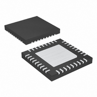
MAX9706ETX+ Maxim Integrated Products, MAX9706ETX+ Datasheet - Page 18

MAX9706ETX+
Manufacturer Part Number
MAX9706ETX+
Description
IC AMP AUDIO 2.3W STER+1 36TQFN
Manufacturer
Maxim Integrated Products
Series
DirectDrive™r
Type
Class Dr
Datasheet
1.MAX9707ETX.pdf
(25 pages)
Specifications of MAX9706ETX+
Output Type
2-Channel (Stereo) with Stereo Headphones and Subwoofer
Max Output Power X Channels @ Load
2.3W x 3 @ 4 Ohm; 95mW x 2 @ 16 Ohm
Voltage - Supply
4.5 V ~ 5.5 V
Features
Depop, Short-Circuit and Thermal Protection, Shutdown
Mounting Type
Surface Mount
Package / Case
36-TQFN Exposed Pad
Lead Free Status / RoHS Status
Lead free / RoHS Compliant
3-Channel, 2.3W, Filterless Class D Amplifiers
with Active Crossover
tantalum-blocking capacitors, the MAX9706 charge
pump requires two small ceramic capacitors, conserv-
ing board space, reducing cost, and improving the fre-
quency response of the headphone amplifier. See the
Output Power vs. Charge-Pump Capacitance graph in
the Typical Operating Characteristics for details on siz-
ing charge-pump capacitors. There is a low DC voltage
on the driver outputs due to amplifier offset. However,
the offset of the MAX9706 is typically 1.7mV, which,
when combined with a 32Ω load, results in less than
53µA of DC current flow to the headphones.
In addition to the cost and size disadvantages of the
DC-blocking capacitors required by conventional head-
phone amplifiers, these capacitors limit the amplifier’s
low-frequency response and can distort the audio sig-
nal (Figure 8). Previous attempts at eliminating the out-
put-coupling capacitors involved biasing the
headphone return (sleeve) to the DC bias voltage of the
headphone amplifiers. This method raises some issues:
1)
2)
When using the headphone jack as a line out to other
equipment, the bias voltage on the sleeve may conflict
with the ground potential from other equipment, result-
ing in possible damage to the drivers.
The MAX9706 features a low-noise charge pump. The
switching frequency of the charge pump is one-half the
switching frequency of the Class D amplifier, regardless
of the operating mode. When SYNC_IN is driven exter-
nally, the charge pump switches at 1/2 f
SYNC_IN = V
spread-spectrum pattern. The nominal switching fre-
quency is well beyond the audio range, and thus does
not interfere with the audio signals, resulting in an SNR of
96dB. The switch drivers feature a controlled switching
speed that minimizes noise generated by turn-on and
turn-off transients. By limiting the switching speed of the
charge pump, the di/dt noise caused by the parasitic
bond wire and trace inductance is minimized. Although
not typically required, additional high-frequency noise
attenuation can be achieved by increasing the size of the
charge-pump reservoir capacitor C2 (see the Functional
Diagram/Typical Operating Circuits). The charge pump is
active in both speaker and headphone modes.
18
______________________________________________________________________________________
The sleeve is typically grounded to the chassis.
Using the midrail biasing approach, the sleeve
must be isolated from system ground, complicat-
ing product design.
During an ESD strike, the driver’s ESD structures
are the only path to system ground. Thus, the dri-
ver must be able to withstand the full ESD strike.
DD
, the charge pump switches with a
SYNC_IN
Charge Pump
. When
Figure 7. Traditional Amplifier Output vs. MAX9706 DirectDrive
Output
Figure 8. Low-Frequency Rolloff
-10
-15
-20
-25
-30
-35
-5
0
10
R
L
CONVENTIONAL AMPLIFIER
= 16Ω
DirectDrive AMPLIFIER
BIASING SCHEME
BIASING SCHEME
FREQUENCY (Hz)
100
DirectDrive
330μF
220μF
100μF
33μF
V
V
GND
+V
SGND
-V
DD
DD
DD
DD
1000
/ 2


