LM4884MHX/NOPB National Semiconductor, LM4884MHX/NOPB Datasheet - Page 16
LM4884MHX/NOPB
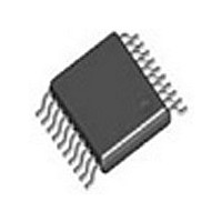
Manufacturer Part Number
LM4884MHX/NOPB
Description
IC AMP AUDIO 2.6W STER 20TSSOP
Manufacturer
National Semiconductor
Series
Boomer®r
Type
Class ABr
Datasheet
1.LM4884MHXNOPB.pdf
(22 pages)
Specifications of LM4884MHX/NOPB
Output Type
2-Channel (Stereo)
Max Output Power X Channels @ Load
2.6W x 2 @ 3 Ohm
Voltage - Supply
3 V ~ 5.5 V
Features
Depop, Differential Inputs, Shutdown, Thermal Protection
Mounting Type
Surface Mount
Package / Case
20-TSSOP Exposed Pad, 20-eTSSOP, 20-HTSSOP
Operational Class
Class-AB
Audio Amplifier Output Configuration
2-Channel Stereo
Output Power (typ)
2.6x2@3OhmW
Audio Amplifier Function
Speaker
Total Harmonic Distortion
0.3@4Ohm@2W%
Single Supply Voltage (typ)
5V
Dual Supply Voltage (typ)
Not RequiredV
Power Supply Requirement
Single
Rail/rail I/o Type
No
Power Supply Rejection Ratio
62dB
Single Supply Voltage (min)
3V
Single Supply Voltage (max)
5.5V
Dual Supply Voltage (min)
Not RequiredV
Dual Supply Voltage (max)
Not RequiredV
Operating Temp Range
-40C to 85C
Operating Temperature Classification
Industrial
Mounting
Surface Mount
Pin Count
20
Package Type
TSSOP
Lead Free Status / RoHS Status
Lead free / RoHS Compliant
Other names
LM4884MHX


www.national.com
Application Information
POWER DISSIPATION
Power dissipation is a major concern when designing a
successful bridged or single-ended amplifier. Equation (2)
states the maximum power dissipation point for a single-
ended amplifier operating at a given supply voltage and
driving a specified output load.
However, a direct consequence of the increased power de-
livered to the load by a bridge amplifier is an increase in the
internal power dissipation point for a bridge amplifier oper-
ating at the same given conditions.
The LM4884 has four operational amplifiers in one package
and the maximum internal power dissipation is four times
that of a single-ended amplifier. From Equation (3), assum-
ing a 5V power supply and an 8Ω load, the maximum power
dissipation point is 2W. The maximum power dissipation
point obtained from Equation (3) must not exceed the power
dissipation predicted by Equation (4):
For the exposed DAP TSSOP package, θ
T
perature T
internal power dissipation supported by the IC packaging. If
the result of Equation (3) is greater than that of Equation (4),
decrease the supply voltage, increase the load impedance,
or reduce the ambient temperature. For a typical application
with a 5V power supply and an 8Ω load, the maximum
ambient temperature that does not violate the maximum
junction temperature is approximately 68˚C. This further as-
sumes that a device is a surface mount part operating
around the maximum power dissipation point. Since internal
power dissipation is a function of output power, higher am-
bient temperatures are allowed as output power decreases.
Refer to the Typical Performance Characteristics curves for
power dissipation information at lower output power levels.
BTL GAIN SELECTION
The LM4884 features four fixed, internally set, BTL voltage
gains: 6dB, 10dB, 15.6dB, and 21.6dB. Select one of the
four gains by applying a logic level signal to the GAIN0
(MSB) and GAIN1 (LSB) digital inputs.
The closed-loop gain of the first amplifier is adjustable, hav-
ing four different gains, whereas two internal 20kΩ resistors
set the second amplifier’s gain at -1. Table 1 below, shows
the state of the two logic inputs required to select one of the
four gain values.
JAMAX
= 150˚C for the LM4884. For a given ambient tem-
P
P
DMAX
A
DMAX
, Equation (4) can be used to find the maximum
= 4 * (V
P
= (V
DMAX
DD
DD
)
= (T
2
/(2π
)
2
/(2π
JMAX
2
R
2
L
R
) Single-Ended
− T
L
) Bridge Mode
A
)/θ
JA
(Continued)
JA
= 41˚C/W.
(2)
(3)
(4)
16
POWER SUPPLY BYPASSING
As with any power amplifier, proper supply bypassing is
critical for low noise performance and high power supply
rejection. The capacitors connected to the bypass and power
supply pins should be placed as close to the LM4884 as
possible. The capacitor connected between the bypass pin
and ground improves the internal bias voltage’s stability,
producing improved PSRR. The improvements to PSRR
increase as the bypass pin capacitor value increases.
Typical applications employ a 5V regulator with 10µF and a
0.1µF filter capacitors that aid in supply stability. Their pres-
ence, however, does not eliminate the need for bypassing
the LM4884’s supply pins. The selection of bypass capacitor
values, especially C
ments, click and pop performance (as explained in theSe-
lecting External Components section), system cost, and
size constraints.
MICRO-POWER SHUTDOWN
The LM4884 features an active-low micro-power shutdown
mode. The voltage applied to the SHUTDOWN pin controls
the LM4884’s shutdown function. Activate micro-power shut-
down by applying 0V to the SHUTDOWN pin. The logic
threshold is typically 0.4V for a logic low and 1.5V for a logic
high. When active, the LM4884’s micro-power shutdown
feature turns off the amplifier’s bias circuitry, disables the
internal V
into a high impedance state. The result is greatly reduced
power supply current. The low 0.1µA typical shutdown cur-
rent is achieved by applying a voltage to the SHUTDOWN
pin that is as near to GND as possible. A voltage that is
greater than GND may increase the shutdown current.
There are a few methods to control the micro-power shut-
down. These include using a single-pole, single-throw switch
(SPST), a microprocessor, or a microcontroller. When using
a switch, connect a 100kΩ pull-down resistor between the
SHUTDOWN pin and GND and the SPST switch between
the SHUTDOWN pin and V
eration by closing the switch. Opening the switch applies
GND to the SHUTDOWN pin, activating micro-power shut-
down. The switch and resistor guarantee that the SHUT-
DOWN pin will not float. This prevents unwanted state
changes. In a system with a microprocessor or a microcon-
troller, use a digital output to apply the active-state voltage to
the SHUTDOWN pin. Driving the SHUTDOWN pin with ac-
tive circuitry eliminates the pull-down resistor.
GAIN 0 GAIN 1
0
0
1
1
Table 1. Gain Settings and Input Resistance
DD
/2 generator, and forces the amplifier outputs
0
1
0
1
B
Selected Gain
, depends on desired PSRR require-
(dB)
15.6
21.6
10
6
DD
. Select normal amplifier op-
Input Resistance
90kΩ
70kΩ
45kΩ
25kΩ
(R
i
)
Related parts for LM4884MHX/NOPB
Image
Part Number
Description
Manufacturer
Datasheet
Request
R

Part Number:
Description:
2.1w Differential Input, Btl Output Stereo Audio Amplifier With Rf Suppression And Shutdown
Manufacturer:
National Semiconductor Corporation
Datasheet:

Part Number:
Description:
IC AMP AUDIO 2.6W STER 20TSSOP
Manufacturer:
National Semiconductor
Datasheet:
Part Number:
Description:
2.1W Differential Input, BTL Output Stereo Audio Amplifier with RF Suppression and Shutdown
Manufacturer:
NSC [National Semiconductor]
Datasheet:
Part Number:
Description:
National Semiconductor [8-Bit D/A Converter]
Manufacturer:
National Semiconductor
Datasheet:
Part Number:
Description:
National Semiconductor [Media Coprocessor]
Manufacturer:
National Semiconductor
Datasheet:
Part Number:
Description:
Digitally Controlled Tone and Volume Circuit with Stereo Audio Power Amplifier, Microphone Preamp Stage and National 3D Sound
Manufacturer:
National Semiconductor
Datasheet:
Part Number:
Description:
Digitally Controlled Tone and Volume Circuit with Stereo Audio Power Amplifier, Microphone Preamp Stage and National 3D Sound
Manufacturer:
National Semiconductor
Datasheet:
Part Number:
Description:
AC97 Rev 2 Codec with Sample Rate Conversion and National 3D Sound
Manufacturer:
National Semiconductor
Part Number:
Description:
Manufacturer:
National Semiconductor
Datasheet:
Part Number:
Description:
Manufacturer:
National Semiconductor
Datasheet:
Part Number:
Description:
General Purpose, Low Voltage, Low Power, Rail-to-Rail Output Operational Amplifiers
Manufacturer:
National Semiconductor
Datasheet:
Part Number:
Description:
8-bit 20 MSPS flash A/D converter.
Manufacturer:
National Semiconductor
Datasheet:
Part Number:
Description:
Low Noise Quad Operational Amplifier
Manufacturer:
National Semiconductor
Datasheet:
Part Number:
Description:
Quad Differential Line Receivers
Manufacturer:
National Semiconductor
Datasheet: