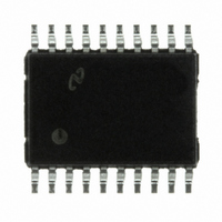
LM4873MT/NOPB National Semiconductor, LM4873MT/NOPB Datasheet - Page 18

LM4873MT/NOPB
Manufacturer Part Number
LM4873MT/NOPB
Description
IC AMP AUDIO PWR 3W STER 20TSSOP
Manufacturer
National Semiconductor
Series
Boomer®r
Type
Class ABr
Datasheet
1.LM4873MTEXNOPB.pdf
(25 pages)
Specifications of LM4873MT/NOPB
Output Type
2-Channel (Stereo) with Stereo Headphones
Max Output Power X Channels @ Load
3W x 2 @ 3 Ohm; 440mW x 2 @ 8 Ohm
Voltage - Supply
2 V ~ 5.5 V
Features
Depop, Input Multiplexer, Shutdown, Thermal Protection
Mounting Type
Surface Mount
Package / Case
20-TSSOP
Lead Free Status / RoHS Status
Lead free / RoHS Compliant
Other names
*LM4873MT
LM4873MT
LM4873MT
www.national.com
Application Information
without clipping or other audible distortion. The choice of
supply voltage must also not create a situation that violates
maximum power dissipation as explained above in the
Power Dissipation section.
After satisfying the LM4873’s power dissipation require-
ments, the minimum differential gain needed to achieve 1W
dissipation in an 8Ω load is found using Equation (10).
Thus, a minimum gain of 2.83 allows the LM4873’s to reach
full output swing and maintain low noise and THD+N perfor-
mance. For this example, let A
The amplifier’s overall gain is set using the input (R
feedback (R
set at 20kΩ, the feedback resistor is found using Equation
(11).
The value of R
The last step in this design example is setting the amplifier’s
−3dB frequency bandwidth. To achieve the desired
pass band magnitude variation limit, the low frequency re-
sponse must extend to at least one-fifth the lower bandwidth
limit and the high frequency response must extend to at least
five times the upper bandwidth limit. The gain variation for
both response limits is 0.17dB, well within the
desired limit. The results are an
and an
As mentioned in the External Components section, R
C
bandpass frequency limit. Find the coupling capacitor’s
value using Equation (12).
The result is
Use a 0.39µF capacitor, the closest standard value.
The product of the desired high frequency cutoff (100kHz in
this example) and the differential gain, AVD, determines the
upper passband response limit. With A
100kHz, the closed-loop gain bandwidth product (GBWP) is
300kHz. This is less than the LM4873’s 3.5MHz GBWP. With
this margin, the amplifier can be used in designs that require
more differential gain while avoiding performance-restricting
bandwidth limitations.
RECOMMENDED PRINTED CIRCUIT BOARD LAYOUT
Figures 4 through 6 show the recommended two-layer PC
board layout that is optimized for the 20-pin MTE-packaged
LM4873 and associated external components. Figures 7
through 11 show the recommended four-layer PC board
layout that is optimized for the 24-pin LQ-packaged LM4873
and associated external components. Figures 12 through 16
show the recommended four-layer PC board layout that is
optimized for the 20-pin micro SMD-packaged LM4873 and
associated external components. These circuits are de-
signed for use with an external 5V supply and 4Ω speakers.
i
create a highpass filter that sets the amplifier’s lower
f
) resistors. With the desired input impedance
f
1/(2π*20kΩ*20Hz) = 0.398µF.
is 30kΩ.
f
H
f
L
= 20kHz*5 = 100kHz.
= 100Hz/5 = 20Hz
C
R
i
f
/R
≥ 1/(2πR
i
= A
VD
VD
= 3.
i
/2
f
L
)
VD
(Continued)
= 3 and f
±
±
0.25dB
0.25dB
i
) and
i
(10)
(12)
(11)
H
and
=
18
These circuit boards are easy to use. Apply 5V and ground to
the board’s V
speakers between the board’s −OUTA and +OUTA and
OUTB and +OUTB pads.
FIGURE 4. Recommended MTE PC Board Layout:
FIGURE 5. Recommended MTE PC Board Layout:
FIGURE 6. Recommended MTE PC Board Layout:
DD
Component-Side Silkscreen
Component-Side Layout
and GND pads, respectively. Connect 4Ω
Bottom-Side Layout
10099393
10099391
10099392


