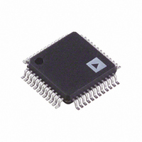
ADAU1592ASVZ Analog Devices Inc, ADAU1592ASVZ Datasheet - Page 15

ADAU1592ASVZ
Manufacturer Part Number
ADAU1592ASVZ
Description
IC AMP AUDIO PWR 24W STER 48TQFP
Manufacturer
Analog Devices Inc
Type
Class Dr
Datasheet
1.ADAU1592ACPZ.pdf
(24 pages)
Specifications of ADAU1592ASVZ
Output Type
2-Channel (Stereo)
Max Output Power X Channels @ Load
24W x 2 @ 4 Ohm
Voltage - Supply
9 V ~ 18 V
Features
Depop, Mute, Short-Circuit and Thermal Protection, Standby
Mounting Type
Surface Mount
Package / Case
48-TQFP Exposed Pad, 48-eTQFP, 48-HTQFP, 48-VQFP
Lead Free Status / RoHS Status
Lead free / RoHS Compliant
Available stocks
Company
Part Number
Manufacturer
Quantity
Price
Company:
Part Number:
ADAU1592ASVZ
Manufacturer:
ADI
Quantity:
340
THEORY OF OPERATION
OVERVIEW
The ADAU1592 is a 2-channel, high performance switching
audio power amplifier. Each of the two Σ-Δ modulators converts
a single-ended analog input into a 2-level PDM output. This
PDM pulse stream is output from the internal full differential
power stage. The ADAU1592 has built-in circuits to suppress the
turn-on and turn-off pop and click. The ADAU1592 also offers
extensive thermal and overcurrent protection circuits.
MODULATOR
The modulator is a 5
stage connected internally. This helps reduce the external
connections. The 5
near full-scale inputs. The modulator gain is optimized at 19 dB
for 15 V operation. The Σ-Δ modulator outputs a pulse density
modulation (PDM) 1-bit stream, which does not produce
distinct sharp peaks and harmonics in the AM band like
conventional fixed-frequency PWM.
The Σ-Δ modulators require feedback to generate PDM stream
with respect to the input. The feedback for the modulators
comes from the power stage. This helps reduce the nonlinearity
in the power stages and achieve excellent THD + N perform-
ance. The feedback also helps in achieving good PSRR. In the
ADAU1592, the feedback from the power stage is internally
connected. This helps reduce the external connections for ease
in PCB layout.
The Σ-Δ modulators operate in a discrete time domain and
Nyquist frequency limit, which is half the sampling frequency.
The modulator uses the master clock of 12.288 MHz. This is
generated by dividing the external clock input by 2. This sets
the f
bandwidth of 22 kHz. The modulator shapes the quantization
noise and transfers it outside the audio band. The noise floor
rises sharply above 20 kHz. This ensures very good signal-to-
noise ratio (SNR) in the audio band of 20 kHz. The 6.144 MHz
bandwidth allows the modulator order to be set around the 5
order. The modulator uses proprietary dynamic hysteresis to
reduce the switching rate or frequency to around 700 kHz.
This reduces the switching losses and achieves good efficiency.
The dynamic hysteresis helps the modulator to continuously
track the change in PVDD and the input level to keep the
modulator stable.
SLICER
The ADAU1592 has a built-in slicer block following the PGA
and before the modulator. The slicer block is essentially a hard
limiter included for limiting the input signal to the modulator.
This, in turn, limits the output power at a given supply voltage.
The slicer in the ADAU1592 is normally inactive at lower input
levels but is activated as soon as the peak input voltage exceeds
the set threshold. The threshold can be set externally by
connecting a resistor from SLC_TH (Pin 24) to ground. This
S
/2 around 6.144 MHz. This is sufficient for the audio
th
-order modulator switches to a lower order
th
-order Σ-Δ with feedback from the power
Rev. A | Page 15 of 24
th
feature allows the user to adjust the slicer to the desired value
and to limit the output power. For input signals higher than the
set threshold, the slicer clips the input signal to the modulator.
This adds distortion due to clipping of the signal input to the
modulator. This is especially helpful in applications where the
output power available needs to be reduced instead of reducing
the supply voltage.
Figure 41 is a plot showing THD + N vs. the input level at 0 dB
PGA, 15 V, and 6 Ω, and demonstrates the difference between a
device with and without the slicer.
Figure 42 depicts the typical output power vs. input at different
slicer settings.
From Figure 42, it can be seen that the slicer effectively reduces
the output power depending on its setting.
Internally, the slicer block receives the input from the PGA.
Figure 43 shows the block for slicer threshold adjust, SLC_TH
(Pin 24).
Figure 42. Typical Output Power vs. Input at Different Slicer Settings
–100
–10
–15
–20
–25
–30
–35
–40
–45
–50
–55
–60
–65
–70
–75
–80
–85
–90
–95
25
20
15
10
–5
5
0
0
0
0
Figure 41. THD + N vs. Input Level @ PGA = 0 dB, 15 V
SLICER DISABLED
0.2
0.2
SLICER 1.17V
SLICER 1.24V
SLICER 1.32V
SLICER 1.1V
0.4
0.4
0.6
0.6
SLICER DISABLED
0.8
0.8
INPUT (V rms)
SLICER 1.32V
SLICER 1.24V
SLICER 1.17V
SLICER 1.10V
INPUT (V rms)
1.0
1.0
1.2
1.2
1.4
1.4
1.6
1.6
ADAU1592
1.8
1.8
2
2
.0
.0


