NJM2113M NJR, NJM2113M Datasheet
Home Integrated Circuits (ICs) Linear - Amplifiers - Audio NJM2113M
Manufacturer Part Number
NJM2113M
Description
IC AUDIO POWER AMP LOW-VOLT 8DMP
Specifications of NJM2113M
Output Type
1-Channel (Mono)
Max Output Power X Channels @ Load
400mW x 1 @ 100 Ohm
Voltage - Supply
2 V ~ 16 V
Features
Standby
Mounting Type
Surface Mount
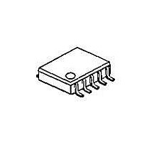
Package / Case
8-DMP
Product
Class-AB
Output Power
400 mW
Available Set Gain
83 dB
Thd Plus Noise
0.6 %
Operating Supply Voltage
3 V, 5 V, 9 V
Supply Current
3.4 mA
Maximum Power Dissipation
500 mW
Maximum Operating Temperature
+ 75 C
Mounting Style
SMD/SMT
Audio Load Resistance
100 Ohms
Input Bias Current (max)
0.2 uA
Input Offset Voltage
0.8 V
Input Signal Type
Differential
Minimum Operating Temperature
- 20 C
Output Signal Type
Differential
Supply Type
Single
Supply Voltage (max)
16 V
Supply Voltage (min)
2 V
Lead Free Status / RoHS Status
Contains lead / RoHS non-compliant
Available stocks
Part Number:
NJM2113M (TE1)
Part Number:
NJM2113M (TE2)
Part Number:
NJM2113M -TE1
Part Number:
NJM2113M -TE1
Part Number:
NJM2113M ��TE1��
■ GENERAL DESCRIPTION
applications, such as in speakerphones.
differential speaker outputs. The closed loop gain is set with two
external resistors. A CD pin permit powering down with muting the
input signal.
■ FEATURES
■ RECOMMENDED OPERATING CONDITIONS
■ PIN CONFIGURATION
■ BLOCK DIAGRAM
Ver.2008-03-07
The NJM2113 is a audio power amplifier designed for telephone
Coupling capacitors to the speaker are not required, as it has
● Wide Operating Voltage
● Low Operating Current
● CD Input to Power Down the IC with Mute
● Low Power-Down Operating Current ( 72µA Typ. )
● Output Power Exceeds 250mW
● Gain Adjustable
● Package Outline
● Bipolar Technology
● Load Impedance
● Differential Gain
● Input Voltage at CD
LOW VOLTAGE AUDIO POWER AMPLIFIER
NJM2113D
NJM2113M
NJM2113V
NJM2113R
( 2~16V )
( 2.7mA Typ. )
( V
(G
DMP8,DIP8,SIP8,SSOP8,VSP8,EMP8
R
G
V
CD
L
VD
VD
+
=6V,R
=0~43dB,Voice Band )
L
8~200Ω
0~43dB ( 5kHz bandwidth )
0~V
=32Ω )
+
Vdc
NJM2113L
■ PACKAGE OUTLINE
NJM2113D
NJM2113L
PIN FUNCTION
1.
2.
3.
4.
5.
6.
7.
8.
CD
V
+V
–V
V
V
GND
V
REF
OUT
+
OUT
IN
IN
1
2
NJM2113M
NJM2113V
NJM2113E
NJM2113R
- 1 -
Related parts for NJM2113M
NJM2113M Summary of contents
... PIN CONFIGURATION NJM2113D NJM2113M NJM2113V NJM2113R ■ BLOCK DIAGRAM Ver.2008-03-07 ■ PACKAGE OUTLINE ( 2~16V ) ( 2.7mA Typ =6V,R =32Ω =0~43dB,Voice Band ) VD DMP8,DIP8,SIP8,SSOP8,VSP8,EMP8 R 8~200Ω 0~43dB ( 5kHz bandwidth ) 0~V Vdc CD NJM2113L NJM2113M NJM2113D NJM2113V NJM2113L NJM2113R NJM2113E PIN FUNCTION REF – OUT + GND OUT ...
... V Output High Level V Output Low Level V Output DC Offset ∆V Input Bias Current Equivalent Resistance Input Voltage Input Voltage Input Resistance R ( note2 ) NJM2113M,NJM2113V : Board ( note3 ) Not specified for NJM2113V,NJM2113R - 2 - RATINGS + V +18 I ± 250 1~4pin )-0 +0 5,8pin )-0 +0 when Power-Down ) ( DIP8 ) 500 ...
APPLICATION CIRCUIT INPUT Power-Down Control ( note ) 1. The NJM2113 is active mode during the CD terminal is Low level ( <0.8V ) and it is stand-by mode during the CD terminal is High level ( >2.0V ) ...
TYPICAL CHARACTERISTICS - 4 - Ver.2008-03-07 ...
TYPICAL CHARACTERISTICS Ver.2008-03- ...
TYPICAL CHARACTERISTICS - 6 - [CAUTION] The specifications on this databook are only given for information , without any guarantee as regards either mistakes or omissions. The application circuits in this databook are described only to show representative usages ...
Related keywords
njm2113 njm2113m njm2153 njm2113e njm2113v njm2113d njm2113v-te1 njm2113m-te1 NJM2113M datasheet NJM2113M data sheet NJM2113M pdf datasheet NJM2113M component NJM2113M part NJM2113M distributor NJM2113M RoHS NJM2113M datasheet download