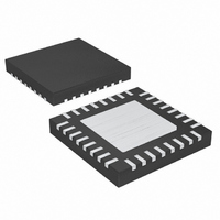
MAX9714ETJ+ Maxim Integrated Products, MAX9714ETJ+ Datasheet - Page 10

MAX9714ETJ+
Manufacturer Part Number
MAX9714ETJ+
Description
IC AMP AUDIO PWR 8W STER 32TQFN
Manufacturer
Maxim Integrated Products
Type
Class Dr
Datasheet
1.MAX9713ETJ.pdf
(18 pages)
Specifications of MAX9714ETJ+
Output Type
2-Channel (Stereo)
Max Output Power X Channels @ Load
8W x 2 @ 16 Ohm
Voltage - Supply
10 V ~ 25 V
Features
Depop, Differential Inputs, Mute, Short-Circuit and Thermal Protection, Shutdown
Mounting Type
Surface Mount
Package / Case
32-TQFN Exposed Pad
Product
Class-D
Output Power
6 W
Common Mode Rejection Ratio (min)
60 dB
Thd Plus Noise
0.07 %
Supply Current
18 mA
Maximum Power Dissipation
2963 mW
Maximum Operating Temperature
+ 85 C
Mounting Style
SMD/SMT
Audio Load Resistance
8 Ohms
Minimum Operating Temperature
- 40 C
Lead Free Status / RoHS Status
Lead free / RoHS Compliant
is very small. Although this movement is small, a speak-
er not designed to handle the additional power can be
damaged. For optimum results, use a speaker with a
series inductance > 30µH. Typical 8Ω speakers exhibit
series inductances in the range of 30µH to 100µH.
Optimum efficiency is achieved with speaker induc-
tances > 60µH.
Table 2 shows the suggested gain settings to attain a
maximum output power from a given peak input voltage
and given load.
The MAX9713/MAX9714 feature an internal, 6V regula-
tor output (V
pin simplifies system design and reduces system cost
by providing a logic voltage high for the MAX9713/
MAX9714 logic pins (G_, FS_). V
a logic voltage high in shutdown mode. Do not apply
V
MAX9714 SHDN pin. Do not apply V
tial to surrounding system components. Bypass REG
with a 6.3V, 0.01µF capacitor to GND.
Unlike a Class AB amplifier, the output offset voltage of
Class D amplifiers does not noticeably increase quies-
cent current draw when a load is applied. This is due to
the power conversion of the Class D amplifier. For
example, an 8mV DC offset across an 8Ω load results
in 1mA extra current consumption in a Class AB device.
In the Class D case, an 8mV offset into 8Ω equates
to an additional power drain of 8µW. Due to the high
efficiency of the Class D amplifier, this represents an
additional quiescent current draw of: 8µW/(V
which is on the order of a few microamps.
6W, Filterless, Spread-Spectrum
Mono/Stereo Class D Amplifiers
Table 2. Gain Settings
10
REG
GAIN (dB)
13.0
16.1
19.1
22.1
13.0
16.1
19.1
22.1
______________________________________________________________________________________
as an input voltage high to the MAX9713/
REG
Internal Regulator Output (V
). The MAX9713/MAX9714 REG output
DIFF INPUT
(V
1.27
0.89
0.63
0.45
0.78
0.54
0.39
0.27
RMS
)
REG
R
L
16
16
16
16
8
8
8
8
REG
Gain Selection
(Ω)
is not available as
Output Offset
as a 6V poten-
DD
THD+N (W)
/100
at 10%
P
OUT
8
8
8
8
6
6
6
6
REG
✕
η),
)
The MAX9713/MAX9714 feature a differential input struc-
ture, making them compatible with many CODECs, and
offering improved noise immunity over a single-ended
input amplifier. In devices such as PCs, noisy digital sig-
nals can be picked up by the amplifier’s input traces.
The signals appear at the amplifiers’ inputs as common-
mode noise. A differential input amplifier amplifies the
difference of the two inputs, any signal common to both
inputs is canceled.
The MAX9713/MAX9714 can be configured as single-
ended input amplifiers by capacitively coupling either
input to GND and driving the other input (Figure 5).
An input capacitor, C
impedance of the MAX9713/MAX9714, forms a high-
pass filter that removes the DC bias from an incoming
signal. The AC-coupling capacitor allows the amplifier
to bias the signal to an optimum DC level. Assuming
zero-source impedance, the -3dB point of the highpass
filter is given by:
Choose C
of interest. Setting f
quency response of the amplifier. Use capacitors
whose dielectrics have low-voltage coefficients, such
as tantalum or aluminum electrolytic. Capacitors with
high-voltage coefficients, such as ceramics, may result
in increased distortion at low frequencies.
Use capacitors with an ESR less than 100mΩ for opti-
mum performance. Low-ESR ceramic capacitors mini-
mize the output resistance of the charge pump. For
best performance over the extended temperature
range, select capacitors with an X7R dielectric.
Figure 5. Single-Ended Input
IN
SINGLE-ENDED
Charge-Pump Capacitor Selection
so f
AUDIO INPUT
-3dB
0.47µF
f
- 3dB
-3dB
is well below the lowest frequency
IN
0.47µF
, in conjunction with the input
=
too high affects the low-fre-
2
Component Selection
π
R C
IN+
IN-
IN IN
1
MAX9713/
MAX9714
Single-Ended Input
Input Amplifier
Differential Input
Input Filter


