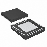
MAX9789CETJ+ Maxim Integrated Products, MAX9789CETJ+ Datasheet - Page 18

MAX9789CETJ+
Manufacturer Part Number
MAX9789CETJ+
Description
IC AMP AUDIO 2W STER AB 32TQFN
Manufacturer
Maxim Integrated Products
Series
DirectDrive™r
Type
Class ABr
Datasheet
1.MAX9789AETJ.pdf
(28 pages)
Specifications of MAX9789CETJ+
Output Type
2-Channel (Stereo) with Stereo Headphones
Max Output Power X Channels @ Load
2W x 2 @ 4 Ohm; 100mW x 2 @ 16 Ohm
Voltage - Supply
4.5 V ~ 5.5 V
Features
Depop, Mute, Short-Circuit and Thermal Protection, Shutdown
Mounting Type
Surface Mount
Package / Case
32-TQFN Exposed Pad
Lead Free Status / RoHS Status
Lead free / RoHS Compliant
The MAX9789 stereo BTL Class AB speaker amplifier
can be configured to drive a mono speaker. Rather
than combining the CODEC’s left- and right-input sig-
nals in a resistive network prior to one channel of the
speaker amplifier input, the transducer itself can be
connected to the BTL speaker amplifier output as
shown in Figure 6. When compared to the resistive net-
work implementation, the configuration in Figure 6 will:
Under normal operating conditions, the MAX9789/
MAX9790 can dissipate a significant amount of power.
The maximum power dissipation for each package is
given in the Absolute Maximum Ratings section under
Continuous Power Dissipation, or can be calculated by
the following equation:
where T
ture, and θ
°C/W as specified in the Absolute Maximum Ratings
section. For example, θ
age is +40.2°C/W for a multilayer PC board.
Windows Vista-Compliant, Stereo Class AB Speaker
Amplifiers and DirectDrive Headphone Amplifiers
Figure 6. Mono Signal Output Configuration for MAX9789
18
1) Eliminate noise pickup by eliminating the high-
2) Eliminate gain error by eliminating any resistive
______________________________________________________________________________________
impedance node at the CODEC’s left- and right-
signal mixing point. SNR performance will be
improved as a result.
mismatch between the external resistance used to
sum the left and right signals and the MAX9789
internal resistance.
CODEC
J(MAX)
Power Dissipation and Heat Sinking
SPKR_OUTR
SPKR_OUTL
JA
LINE_OUTR
LINE_OUTL
P
DISSPKG MAX
is the reciprocal of the derating factor in
is +150°C, T
Mono Speaker Configuration
C
C
C
C
IN1
IN1
IN2
IN2
(
JA
SPKR_INL
SPKR_INR
HP_INL
HP_INR
for the 32-pin TQFN-EP pack-
)
=
A
MAX9789
T
is the ambient tempera-
J MAX
(
θ
OUTL+
OUTR+
OUTR-
OUTL-
JA
HPR
HPL
)
−
T
A
The increase in power delivered by the BTL configura-
tion directly results in an increase in internal power dis-
sipation over the single-ended configuration. The
maximum power dissipation for a given V
given by the following equation:
If the power dissipation for a given application exceeds
the maximum allowed for a given package, either reduce
V
temperature, or add heat sinking to the device. Large
output, supply, and ground PC board traces improve the
maximum power dissipation in the package.
Thermal-overload protection limits total power dissipa-
tion in these devices. When the junction temperature
exceeds +150°C, the thermal-protection circuitry dis-
ables the amplifier output stage. The amplifiers are
enabled once the junction temperature cools by +15°C.
This results in a pulsing output under continuous ther-
mal-overload conditions as the device heats and cools.
The MAX9789/MAX9790 have separate supply pins for
each portion of the device, allowing for the optimum
combination of headroom and power dissipation and
noise immunity. The speaker amplifiers are powered
from PV
phone amplifiers are powered from HPV
HPV
fiers and ranges from 3V to 5.5V. PV
supply of the headphone amplifiers. Connect PV
CPV
CPV
potential as HPV
age at CPV
CPV
device is powered by V
The MAX9789/MAX9790 have separate supply pins for
each portion of the device, allowing for the optimum
combination of headroom and power dissipation and
noise immunity.
The speaker amplifiers are powered from PV
ranges from 4.5V to 5.5V. Bypass PV
capacitor to PGND. Note additional bulk capacitance is
required at the device if long input traces between
PV
DD
DD
, increase load impedance, decrease the ambient
DD
DD
SS
SS
and the power source are used.
. The internal LDO and the remainder of the
Speaker Amplifier Power-Supply Input (PV
. The charge pump is powered by CPV
ranges from 3V to 5.5V and should be the same
DD
is the positive supply of the headphone ampli-
. PV
Output Power (Speaker Amplifier)
DD
DD
, and the resulting voltage appears at
DD
P
ranges from 4.5V to 5.5V. The head-
DISS MAX
. The charge pump inverts the volt-
(
DD
.
)
Component Selection
=
2
π
V
2
DD
R
Power Supplies
L
Supply Bypassing
2
SS
DD
is the negative
DD
DD
with a 0.1µF
and load is
and PV
DD
. PV
SS
DD
DD
SS
DD
to
)
.
.


