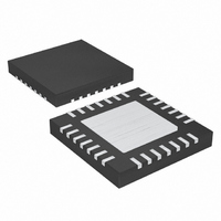
MAX9850ETI+T Maxim Integrated Products, MAX9850ETI+T Datasheet - Page 2

MAX9850ETI+T
Manufacturer Part Number
MAX9850ETI+T
Description
IC AMP AUDIO .095W STER 28TQFN
Manufacturer
Maxim Integrated Products
Series
DirectDrive™r
Type
Class ABr
Datasheet
1.MAX9850ETI.pdf
(36 pages)
Specifications of MAX9850ETI+T
Output Type
Headphones, 2-Channel (Stereo)
Max Output Power X Channels @ Load
95mW x 2 @ 16 Ohm
Voltage - Supply
1.8 V ~ 3.6 V
Features
DAC, Depop, Digital Inputs, I²C, I²S, Line Level Inputs & Outputs, Mute, Shutdown, Volume Control
Mounting Type
Surface Mount
Package / Case
28-WQFN Exposed Pad, 28-HWQFN
Lead Free Status / RoHS Status
Lead free / RoHS Compliant
ABSOLUTE MAXIMUM RATINGS
(Voltages with respect to AGND.)
DV
AV
SV
SV
DGND, PGND........................................................-0.3V to +0.3V
BCLK, LRCLK, HPS, SDIN.......................-0.3V to (DV
GPIO, MCLK.............................................................-0.3V to +4V
REF, PREG ...............................................-0.3V to (AV
NREG ........................................................+0.3V to (SV
SDA, SCL, ADD ........................................................-0.3V to +4V
INL, INR .......................................................................-2V to +2V
HPR, HPL.....................................(SV
ELECTRICAL CHARACTERISTICS
(DV
R
T
Stereo Audio DAC with DirectDrive
Headphone Amplifier
Stresses beyond those listed under “Absolute Maximum Ratings” may cause permanent damage to the device. These are stress ratings only, and functional
operation of the device at these or any other conditions beyond those indicated in the operational sections of the specifications is not implied. Exposure to
absolute maximum rating conditions for extended periods may affect device reliability.
2
Analog Supply Voltage
Digital Supply Voltage
Analog Supply Current
Digital Supply Current
Analog Shutdown Current
Digital Shutdown Current
Shutdown to Full Operation
(Note 2)
Power-On to Full Operation
(Note 2)
DAC PERFORMANCE/LINE OUTPUTS (Note 3)
0dBFS Output Voltage
Dynamic Range (Note 4)
Signal-to-Noise Ratio
(Note 5)
MAX
LOAD_HP
SS
SS
DD
DD
DD
_______________________________________________________________________________________
, PV
, unless otherwise noted. Typical specifications at T
Referenced to PV
, AV
Referenced to PV
= AV
SS
DD
= 32Ω to AGND, R
PARAMETER
...............................................................-4V to +0.3V
DD
, PV
= PV
DD
..................................................-0.3V to +4V
DD
SS
DD
= 3.0V, AGND = DGND = PGND = 0V, C1 = 0.47µF, C2 = 2.2µF, C
.....................................-0.3V to +0.3V
....................................-0.3V to +0.3V
LOAD_OUT
SS
SYMBOL
V
AI
DI
AV
- 0.3V) to (AV
PV
DV
OUT_FS
AI
DI
t
SNR
t
= 10kΩ to AGND, f
SHDN
PON
SHDN
DR
ON
DD
DD
DD
DD
DD
,
AV
Full operation (Note 2),
no headphone or line
output load
Full operation (Note 2),
headphones disabled
Full operation (Note 2),
no line output load
I
Static digital interface, D
AV
AV
Unweighted
A-weighted
AV
AV
AVDD
DD
DD
DD
DD
DD
DD
DD
DD
SS
+ 0.3V)
+ 0.3V)
+ 0.3V)
= PV
= 3.0V
= 1.8V
= 1.8V, unweighted
= 1.8V, A-weighted
+ I
A
- 0.3V)
= +25°C, unless otherwise noted.) (Note 1)
PVDD
LRCLK
DD
, A
CONDITIONS
= 48kHz, f
VDD
OUTL, OUTR .............................(NREG - 0.3V) to (PREG + 0.3V)
C1N ............................................(PV
C1P ............................................(PGND - 0.3V) to (PV
Current Into/Out of Any Pin ...............................................100mA
Duration of HPL, HPR, OUTL,
Continuous Power Dissipation (T
Junction Temperature ......................................................+150°C
Operating Temperature Range ...........................-40°C to +85°C
Storage Temperature Range .............................-65°C to +150°C
Lead Temperature (soldering, 10s) .................................+300°C
= P
28-Pin Thin QFN (derate 35.7mW/°C above +70°C) .....2857mW
OUTR Short Circuit to AGND .................................Continuous
VDD
VDD
MCLK
AV
AV
AV
AV
DV
DV
= 1.8V
= 1.8V
DD
DD
DD
DD
DD
DD
= 12.288MHz, volume set to -9.5dB, T
= 1.8V
= 3.0V
= 1.8V
= 3.0V
= 1.8V
= 3.0V
NREG
1.85
MIN
1.8
1.8
82
= C
A
PREG
= +70°C)
SS
TYP
3.75
1.95
87.5
87.5
5.5
5.9
3.5
2.1
3.8
1.5
0.3
1.3
1.4
- 0.3V) to (PGND + 0.3V)
88
91
88
91
= C
REF
MAX
2.05
= 1µF to AGND,
3.6
3.6
7.7
5.3
2.9
10
5
A
DD
= T
UNITS
+ 0.3V)
V
mA
mA
ms
ms
MIN
µA
µA
dB
dB
P-P
V
V
to


