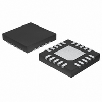
MAX9710ETP+ Maxim Integrated Products, MAX9710ETP+ Datasheet - Page 2

MAX9710ETP+
Manufacturer Part Number
MAX9710ETP+
Description
IC AMP AUDIO PWR 3W STER 20TQFN
Manufacturer
Maxim Integrated Products
Type
Class ABr
Datasheet
1.MAX9711ETCT.pdf
(13 pages)
Specifications of MAX9710ETP+
Output Type
2-Channel (Stereo)
Max Output Power X Channels @ Load
3W x 2 @ 3 Ohm
Voltage - Supply
4.5 V ~ 5.5 V
Features
Depop, Mute, Shutdown, Thermal Protection
Mounting Type
Surface Mount
Package / Case
20-TQFN Exposed Pad
Lead Free Status / RoHS Status
Lead free / RoHS Compliant
ABSOLUTE MAXIMUM RATINGS
V
PV
PGND to GND.....................................................................±0.3V
All Other Pins to GND.................................-0.3V to (V
Continuous Input Current (into any pin
Continuous Power Dissipation (T
3W Mono/Stereo BTL Audio Power Amplifiers
with Shutdown
Stresses beyond those listed under “Absolute Maximum Ratings” may cause permanent damage to the device. These are stress ratings only, and functional
operation of the device at these or any other conditions beyond those indicated in the operational sections of the specifications is not implied. Exposure to
absolute maximum rating conditions for extended periods may affect device reliability.
ELECTRICAL CHARACTERISTICS
(V
noted. Typical values are at T
2
Note 1: All devices are 100% production tested at +25°C. All temperature limits are guaranteed by design.
Note 2: PSSR is specified with the amplifier inputs connected to GND through R
Supply Voltage Range
Quiescent Supply Current
(I
Shutdown Supply Current
Turn-On Time
Thermal Shutdown Threshold
Thermal Shutdown Hysteresis
OUTPUT AMPLIFIERS
Output Offset Voltage
Power-Supply Rejection Ratio
Output Power
Total Harmonic Distortion Plus
Noise
Signal-to-Noise Ratio
Slew Rate
Maximum Capacitive Load Drive
Crosstalk
BIAS VOLTAGE (BIAS)
BIAS Voltage
Output Resistance
DIGITAL INPUTS (MUTE, SHDN)
Input Voltage High
Input Voltage Low
Input Leakage Current
DD
12-Pin Thin QFN (derate 16.9mW/°C above +70°C) ....1349mW
DD
except power supply and output pins).........................±20mA
DD
VDD
_______________________________________________________________________________________
to GND, PGND ...............................................................+6V
= PV
to V
+ I
PVDD
DD
PARAMETER
DD
.......................................................................±0.3V
= 5.0V, V
)
GND
= V
A
= +25°C.) (Note 1)
A
PGND
= +70°C)
V
SYMBOL
DD
THD+N
I
R
PSRR
V
P
= V
SHDN
SNR
V
I
t
V
V
SR
C
BIAS
BIAS
OUT
I
DD
ON
/PV
OS
IN
IH
IL
L
MUTE
DD
= 0V, V
Inferred from PSRR test
MAX9710
MAX9711
SHDN = GND
C
C
V
V
(Note 2)
f
THD+N < 1%
f
22Hz to 22kHz
R
No sustained oscillations
f
IN
IN
IN
OUT_+
RIPPLE
L
BIAS
BIAS
= 8Ω, V
= 1kHz,
= 1kHz, BW =
= 10kHz
DD
= 1µF (10% of final value)
= 0.1µF (10% of final value)
+ 0.3V)
SHDN
- V
= 200mV
OU T
OUT_-
= 5V, R
= 2.8V
CONDITIONS
, A
P-P
V
RM S
Operating Temperature Range............................-40°C to +85°C
Storage Temperature Range .............................-65°C to +150°C
Junction Temperature ......................................................+150°C
Lead Temperature (soldering, 10s) .................................+300°C
= 2
IN
20-Pin Thin QFN (derate 20.8mW/°C above +70°C) ....1667mW
V
f = 1kHz
f = 20kHz
R
R
R
P
P
DD
L
L
L
OUT
OUT
= R
, BW = 22H z to 22kH z
= 8Ω
= 4Ω
= 3Ω
= 4.5V to 5.5V
F
= 1.2W, R
= 2W, 4Ω
= 15kΩ, R
IN
and C
L
= 8Ω
L
IN
= ∞. T
.
A
2.35
MIN
4.5
1.1
= T
82
2
MIN
0.005
to T
TYP
0.01
300
160
100
0.5
1.4
2.6
1.6
2.5
12
30
15
±2
87
74
95
77
50
7
3
1
MAX
, unless otherwise
MAX
2.65
±14
5.5
0.8
30
17
30
±1
UNITS
V/µs
mA
ms
mV
µA
dB
dB
dB
kΩ
µA
°C
°C
nF
W
%
V
V
V
V


