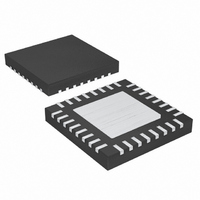
MAX9789CETJ+T Maxim Integrated Products, MAX9789CETJ+T Datasheet - Page 2

MAX9789CETJ+T
Manufacturer Part Number
MAX9789CETJ+T
Description
IC AMP AUDIO 2W STER AB 32TQFN
Manufacturer
Maxim Integrated Products
Series
DirectDrive™r
Type
Class ABr
Datasheet
1.MAX9789AETJ.pdf
(28 pages)
Specifications of MAX9789CETJ+T
Output Type
2-Channel (Stereo) with Stereo Headphones
Max Output Power X Channels @ Load
2W x 2 @ 4 Ohm; 100mW x 2 @ 16 Ohm
Voltage - Supply
4.5 V ~ 5.5 V
Features
Depop, Mute, Short-Circuit and Thermal Protection, Shutdown
Mounting Type
Surface Mount
Package / Case
32-TQFN Exposed Pad
Lead Free Status / RoHS Status
Lead free / RoHS Compliant
Supply Voltage (V
GND to PGND, CPGND ......................................................±0.3V
CPV
HPR, HPL to GND ...............................................................±3.0V
Any Other Pin .............................................-0.3V to (V
Duration of OUT_+, OUT_- Short Circuit
Duration of Short Circuit between OUT_+, OUT_-
Duration of Short Circuit between HPR, HPL and GND,
Continuous Current (PV
Continuous Current (CPV
Windows Vista-Compliant, Stereo Class AB Speaker
Amplifiers and DirectDrive Headphone Amplifiers
ABSOLUTE MAXIMUM RATINGS
ELECTRICAL CHARACTERISTICS
(V
(MAX9789 only) = 0V, I
V
2
Note 1: Package thermal resistances were obtained using the method described in JEDEC specification JESD51-7 using a four-
Stresses beyond those listed under “Absolute Maximum Ratings” may cause permanent damage to the device. These are stress ratings only, and functional
operation of the device at these or any other conditions beyond those indicated in the operational sections of the specifications is not implied. Exposure to
absolute maximum rating conditions for extended periods may affect device reliability.
GENERAL
Supply Voltage
Headphone Supply Voltage
Quiescent Current
Shutdown Current
Bias Voltage
Shutdown to Full Operation
Gain Switching Time
Channel-to-Channel Gain
Tracking
SPEAKER AMPLIFIER
Output Power
Total Harmonic Distortion Plus
Noise
GAIN2
CPV
to GND or PV
and LDO_OUT.........................................................Continuous
V
V
DD
SS
DD,
_______________________________________________________________________________________
SS
= PV
DD
or HPV
, C1N, V
HPV
= 5V (A
layer board. For detailed information on package thermal considerations, refer to www.maxim-ic.com/thermal-tutorial.
to GND) ..................................................-0.3V to +6.0V
DD
PARAMETER
DD
DD
, LDO_OUT, HPR, HPL) .............................850mA
= CPV
SS
DD
VSP
..........................................................Continuous
DD
to GND......................................-6.0V to +0.3V
......................................................Continuous
= 10dB, A
, PV
DD
DD
= HPV
LDO_OUT
DD
DD
, OUT_+, OUT_-, PGND).............1.7A
, HPV
, C1N, C1P, CPV
VHP
DD
DD
= 3.5dB), T
(MAX9789 only) = 0, C1 = C2 = C
= HP_EN = V
,
V
SYMBOL
DD
CPV
THD+N
HPV
I
V
P
SHDN
t
t
I
SON
BIAS
, PV
SW
OUT
DD
DD
DD
SS
DD
A
,
, PV
= T
LDO_EN
Guaranteed by PSRR and LDO Line
Regulation Tests
Guaranteed by PSRR Test
SPKR_EN = V
MAX9789A/MAX9789C/MAX9790A
MAX9789B/MAX9790B
THD+N = 1%, f = 1kHz,
T
R
R
MIN
SS
A
L
L
DD
= +25°C
= 8Ω, P
= 4Ω, P
,
1 (MAX9789)
1 (MAX9790)
to T
SPKR_EN
+ 0.3V)
(MAX9789 only) = +5V, V
MAX
1
0
0
OUT
OUT
, unless otherwise noted. Typical values are at T
DD
CONDITIONS
= 1W, f = 1kHz
= 1W, f = 1kHz
, HP_EN = LDO_EN = GND
Continuous Input Current (all other pins) .........................±20mA
Continuous Power Dissipation (T
Operating Temperature Range ...........................-40°C to +85°C
Junction Temperature ......................................................+150°C
Storage Temperature Range .............................-65°C to +150°C
Lead Temperature (soldering, 10s) .................................+300°C
BIAS
32-Pin Thin QFN Single-Layer Board
(derate 18.6mW/°C above +70°C) ..............................1489mW
32-Pin Thin QFN Multilayer Board
(derate 24.9 mW/°C above +70°C) .............................1990mW
θ
θ
θ
θ
JA
JC
JA
JC
= 1µF. R
...........................................................................53.7°C/W
...........................................................................19.9°C/W
...........................................................................40.2°C/W
...........................................................................19.9°C/W
0 (MAX9789)
0 (MAX9790)
HP_EN
GND
1
0
1
R
R
L
L
L
= ∞, unless otherwise specified, V
= V
= 4Ω
= 8Ω
PGND
= V
MIN
4.5
3.0
1.7
CPGND
A
= +70°C)
0.002
0.004
±0.1
TYP
100
0.1
0.3
0.3
1.8
14
18
25
10
= SPKR_EN = V
7
2
1
A
= +25°C.) (Note 2)
MAX
5.5
5.5
0.4
1.9
13
29
40
6
6
GAIN1
LDO_SET
UNITS
mA
mA
ms
dB
µA
µA
µs
W
%
V
V
V
= 0,


