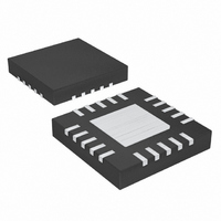
MAX9701ETG+ Maxim Integrated Products, MAX9701ETG+ Datasheet - Page 12

MAX9701ETG+
Manufacturer Part Number
MAX9701ETG+
Description
IC AMP AUDIO PWR 2.2W D 24TQFN
Manufacturer
Maxim Integrated Products
Type
Class Dr
Datasheet
1.MAX9701EBPTG45.pdf
(22 pages)
Specifications of MAX9701ETG+
Output Type
2-Channel (Stereo)
Max Output Power X Channels @ Load
2.2W x 2 @ 4 Ohm
Voltage - Supply
2.5 V ~ 5.5 V
Features
Depop, Differential Inputs, Short-Circuit and Thermal Protection, Shutdown
Mounting Type
Surface Mount
Package / Case
24-TQFN Exposed Pad
Product
Class-D
Output Power
1.3 W
Common Mode Rejection Ratio (min)
66 dB
Thd Plus Noise
0.1 %
Supply Current
6.3 mA
Maximum Power Dissipation
1666.7 mW
Maximum Operating Temperature
+ 85 C
Mounting Style
SMD/SMT
Audio Load Resistance
8 Ohms
Minimum Operating Temperature
- 40 C
Amplifier Class
D
No. Of Channels
2
Supply Voltage Range
2.5V To 5.5V
Load Impedance
8ohm
Operating Temperature Range
-40°C To +85°C
Amplifier Case Style
TQFN
Rohs Compliant
Yes
Lead Free Status / RoHS Status
Lead free / RoHS Compliant
The MAX9701 features a unique spread-spectrum
mode that flattens the wideband spectral components,
improving EMI emissions that may be radiated by the
speaker and cables. This mode is enabled by setting
SYNC = V
quency varies randomly by ±60kHz around the center
frequency (1.2MHz). The modulation scheme remains
the same, but the period of the sawtooth waveform
changes from cycle to cycle (Figure 2). Instead of a
large amount of spectral energy present at multiples of
the switching frequency, the energy is now spread over
a bandwidth that increases with frequency. Above a
few megahertz, the wideband spectrum looks like white
noise for EMI purposes (Figure 3). A proprietary amplifi-
er topology ensures this does not corrupt the noise
floor in the audio bandwidth.
The SYNC input allows the MAX9701 to be synchronized
to a user-defined clock, or another Maxim Class D ampli-
fier, creating a fully synchronous system, minimizing
clock intermodulation, and allocating spectral compo-
nents of the switching harmonics to insensitive frequency
bands. Applying a TTL clock signal between 1000kHz
and 1600kHz to SYNC synchronizes the MAX9701. The
period of the SYNC clock can be randomized, allowing
the MAX9701 to be synchronized to another Maxim Class
D amplifier operating in SSM mode.
1.3W, Filterless, Stereo Class D Audio
Power Amplifier
Figure 3. MAX9701 with 76mm of Speaker Cable with TDK
Common-Mode Choke: TDK ACM4532-801-20-X
12
50.0
45.0
40.0
35.0
30.0
25.0
20.0
15.0
10.0
5.0
0.0
30
______________________________________________________________________________________
DD
60
(Table 1). In SSM mode, the switching fre-
80
100
Synchronous Switching Mode
120
Spread-Spectrum (SSM) Mode
140
FREQUENCY (MHz)
160
180
200
220
240
260
SYNC
280
300
SYNC_OUT allows several MAX9701s as well as other
Class D amplifiers (such as the MAX9700) to be cas-
caded. The synchronized output minimizes interfer-
ence due to clock intermodulation caused by the
switching spread between single devices. Using
SYNC_OUT, the modulation scheme remains the same
and audio reproduction is not affected by changing the
switching frequency.
The MAX9701 uses Maxim’s unique modulation scheme
that eliminates the LC filter required by traditional class D
amplifiers, improving efficiency, reducing component
count, conserving board space and system cost.
Conventional Class D amplifiers output a 50% duty cycle,
180° out-of-phase square wave when no signal is pre-
sent. With no filter, the square wave appears across the
load as a DC voltage, resulting in finite load current,
which increases power consumption especially when
idling. When no signal is present at the input of the
MAX9701, the amplifiers will output an in-phase square
wave as shown in Figure 4. Because the MAX9701 drives
the speaker differentially, the two outputs cancel each
other, resulting in no net idle mode voltage across the
speaker, minimizing power consumption.
Efficiency of a Class D amplifier is due to the switching
operation of the output stage transistors. In a Class D
amplifier, the output transistors act as current-steering
switches and consume negligible additional power.
Any power loss associated with the Class D output
stage is mostly due to the I
resistance and quiescent-current overhead.
Figure 4. MAX9701 Outputs with No Input Signal
V OUT_+ - V OUT_- = 0V
Filterless Modulation/Common-Mode Idle
V IN_ = 0V
OUT_+
OUT_-
2
R loss of the MOSFET on-
Efficiency
SYNC_OUT


