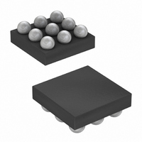
MAX9716EBL+TG45 Maxim Integrated Products, MAX9716EBL+TG45 Datasheet - Page 2

MAX9716EBL+TG45
Manufacturer Part Number
MAX9716EBL+TG45
Description
IC AMP AUDIO PWR 1.4W MONO 9UCSP
Manufacturer
Maxim Integrated Products
Type
Class ABr
Datasheet
1.MAX9716ETAT.pdf
(21 pages)
Specifications of MAX9716EBL+TG45
Output Type
1-Channel (Mono)
Max Output Power X Channels @ Load
1.4W x 1 @ 4 Ohm
Voltage - Supply
2.7 V ~ 5.5 V
Features
Depop, Differential Inputs, Shutdown, Thermal Protection
Mounting Type
Surface Mount
Package / Case
9-UCSP®
Lead Free Status / RoHS Status
Lead free / RoHS Compliant
ABSOLUTE MAXIMUM RATINGS
Supply Voltage (V
Any Other Pin to GND ...............................-0.3V to (V
IN_, BIAS, SHDN, BTL/SE Continuous Current...................20mA
OUT_ Short-Circuit Duration to GND or V
Continuous Power Dissipation (T
Low-Cost, Mono, 1.4W BTL Audio
Power Amplifiers
Stresses beyond those listed under “Absolute Maximum Ratings” may cause permanent damage to the device. These are stress ratings only, and functional
operation of the device at these or any other conditions beyond those indicated in the operational sections of the specifications is not implied. Exposure to
absolute maximum rating conditions for extended periods may affect device reliability.
ELECTRICAL CHARACTERISTICS—5V Supply
(V
BTL/SE = GND (MAX9717_), R
2
Supply Voltage
Quiescent Supply Current
Shutdown Supply Current
SHDN Threshold
BTL/SE Threshold
Common-Mode Bias Voltage
Output Offset Voltage
Power-Supply Rejection Ratio
Output Power
Total Harmonic Distortion Plus
Noise
Output Noise Density
Signal-to-Noise Ratio
CC
8-Pin TDFN (derate 24.4mW/°C above +70°C) .........1951mW
8-Pin µMAX (derate 10.3mW/°C above +70°C) ...........825mW
_______________________________________________________________________________________
= 5V, GND = 0, SHDN = V
PARAMETER
CC
to GND) ..................................-0.3V to +6V
L
CC
A
= ∞ connected between OUT+ and OUT-. Typical values are at T
= +70°C)
, T
A
SYMBOL
THD+N
CC
= +25°C. C
I
V
PSRR
P
SHDN
SNR
V
V
I
V
V
V
V
BIAS
OUT
CC
e
CC
OS
IH
IH
IL
IL
(Note 1)...Continuous
n
Inferred by PSRR test
V
T
SHDN = GND
(Note 4)
V
V
V
V
R
R
R
R
mode), THD+N = 1%, f
A
P
f
THD+N = 1%
IN
BIAS
A
IN-
IN-
CC
IN+
RIPPLE
OUT
L
L
L
L
V
CC
= 8Ω (Note 6)
= -40°C to +85°C
= 8Ω, THD+N = 1%, f
= 4Ω, THD+N = 1%, f
= 16Ω, BTL/SE = V
= 6dB, R
= 10kHz
= V
= V
= 2.7V to 5.5V
= V
= 1µF, R
= 0.5W (Note 8)
+ 0.3V)
IN+
OUT+
= 200mV
BIAS
= V
L
,
, V
= 8Ω, f
IN
CONDITIONS
BIAS
IN+
= R
P-P
= V
Operating Temperature Range ..........................-40°C to +85°C
Maximum Junction Temperature ....................................+150°C
Storage Temperature Range .............................-65°C to +150°C
Lead Temperature (soldering, 10s) .................................+300°C
Bump Temperature (soldering)........................................+235°C
(Note 3),
,
F
IN
CC
9-Bump UCSP (derate 5.2mW/°C above 70°C) ...........412mW
= 20kΩ (MAX9716/MAX9717A), IN+ = BIAS (MAX9716),
BIAS
IN
= 1kHz,
DC, V
f = 217Hz
f = 1kHz
IN
IN
(single-ended
= 1kHz
= 1kHz (Note 7)
= 1kHz (Note 7)
(Note 5)
BIAS
= 1.5V
V
0.9 x
- 6%
A
MIN
V
2.7
1.2
CC
0.8
60
CC
= +25°C.) (Note 2)
/2
V
0.155
0.024
TYP
0.01
106
105
CC
4.3
1.1
1.4
±7
80
61
73
/2
V
+ 6%
MAX
0.7 x
V
±15
CC
5.5
0.4
8
1
CC
/2
nV/√Hz
UNITS
mA
mV
dB
dB
µA
W
%
V
V
V
V


