NCP4894MNR2G ON Semiconductor, NCP4894MNR2G Datasheet - Page 11
NCP4894MNR2G
Manufacturer Part Number
NCP4894MNR2G
Description
IC AMP AUDIO PWR 1W DIFF 10-DFN
Manufacturer
ON Semiconductor
Type
Class ABr
Datasheet
1.NCP4894DMR2G.pdf
(19 pages)
Specifications of NCP4894MNR2G
Output Type
1-Channel (Mono)
Max Output Power X Channels @ Load
1.8W x 1 @ 8 Ohm
Voltage - Supply
2.2 V ~ 5.5 V
Features
Depop, Differential Inputs, Short-Circuit and Thermal Protection, Shutdown
Mounting Type
Surface Mount
Package / Case
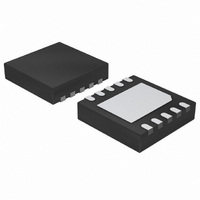
10-VFDFN Exposed Pad
Operational Class
Class-AB
Audio Amplifier Output Configuration
1-Channel Mono
Output Power (typ)
1.08x1@8OhmW
Audio Amplifier Function
Speaker
Total Harmonic Distortion
0.006@8Ohm@1000mW%
Single Supply Voltage (typ)
3/5V
Dual Supply Voltage (typ)
Not RequiredV
Power Supply Requirement
Single
Rail/rail I/o Type
No
Power Supply Rejection Ratio
85dB
Single Supply Voltage (min)
2.2V
Single Supply Voltage (max)
5.5V
Dual Supply Voltage (min)
Not RequiredV
Dual Supply Voltage (max)
Not RequiredV
Operating Temp Range
-40C to 85C
Operating Temperature Classification
Industrial
Mounting
Surface Mount
Pin Count
10
Lead Free Status / RoHS Status
Lead free / RoHS Compliant
Other names
NCP4894MNR2G
NCP4894MNR2GOSTR
NCP4894MNR2GOSTR
Available stocks
Company
Part Number
Manufacturer
Quantity
Price
Company:

Part Number:
NCP4894MNR2G
Manufacturer:
ON Semiconductor
Quantity:
500


700
600
500
400
300
200
100
0.25
0.15
0.05
0.7
0.6
0.5
0.4
0.3
0.2
0.1
0.2
0.1
0
0
0
Figure 29. Power Derating − 9−Pin Flip−Chip CSP
0
0
0
200 mm
P
for VP = 5 V,
R
Figure 25. Power Dissipation versus Output
Figure 27. Power Dissipation versus Output
Dmax
L
= 8 W
20
= 633 mW
0.2
2
T
50 mm
A
40
, AMBIENT TEMPERATURE (°C)
0.1
P
P
out
out
2
0.4
, OUTPUT POWER (W)
, OUTPUT POWER (W)
60
VP = 5 V
R
F = 1 kHz
THD + N < 0.1%
L
= 8 W
Power
VP = 3 V
R
F = 1 kHz
THD + N < 0.1%
Power
L
80
0.6
0.2
= 8 W
TYPICAL PERFORMANCE CHARACTERISTICS
PCB Heatsink Area
500 mm
100
0.8
120
2
0.3
1
140
http://onsemi.com
160
NCP4894
1.2
0.4
11
0.35
0.25
0.15
0.05
180
160
140
120
100
0.25
0.15
0.05
0.4
0.3
0.2
0.1
80
60
40
0.3
0.2
0.1
0
0
50
0
0
Figure 30. Maximum Die Temperature versus
VP = 2.6 V
Figure 28. Power Dissipation versus Output
Figure 26. Power Dissipation versus Output
0.05
VP = 3.3 V
VP = 4.2 V
100
0.1
0.1
R
PCB HEATSINK AREA (mm
VP = 5 V
P
L
P
PCB Heatsink Area
out
= 4 W
R
out
VP = 2.6 V
F = 1 kHz
THD + N < 0.1%
L
, OUTPUT POWER (W)
, OUTPUT POWER (W)
0.15
= 8 W
Maximum Die Temperature 150°C
150
VP = 3.3 V
R
F = 1 kHz
THD + N < 0.1%
0.2
L
Power
= 8 W
Power
0.2
200
0.3
0.25
2
0.3
)
250
0.4
0.35
300
0.5
0.4
Related parts for NCP4894MNR2G
Image
Part Number
Description
Manufacturer
Datasheet
Request
R

Part Number:
Description:
Differential Audio Power Amplifier
Manufacturer:
ON Semiconductor
Datasheet:

Part Number:
Description:
EVAL BOARD FOR NCP4894FC
Manufacturer:
ON Semiconductor
Datasheet:
Part Number:
Description:
ON Semiconductor [VOLTAGE REGULATOR]
Manufacturer:
ON Semiconductor
Datasheet:
Part Number:
Description:
357-036-542-201 CARDEDGE 36POS DL .156 BLK LOPRO
Manufacturer:
ON Semiconductor
Datasheet:
Part Number:
Description:
357-036-542-201 CARDEDGE 36POS DL .156 BLK LOPRO
Manufacturer:
ON Semiconductor
Datasheet:
Part Number:
Description:
357-036-542-201 CARDEDGE 36POS DL .156 BLK LOPRO
Manufacturer:
ON Semiconductor
Datasheet:
Part Number:
Description:
357-036-542-201 CARDEDGE 36POS DL .156 BLK LOPRO
Manufacturer:
ON Semiconductor
Datasheet:
Part Number:
Description:
357-036-542-201 CARDEDGE 36POS DL .156 BLK LOPRO
Manufacturer:
ON Semiconductor
Datasheet:
Part Number:
Description:
357-036-542-201 CARDEDGE 36POS DL .156 BLK LOPRO
Manufacturer:
ON Semiconductor
Datasheet:
Part Number:
Description:
357-036-542-201 CARDEDGE 36POS DL .156 BLK LOPRO
Manufacturer:
ON Semiconductor
Datasheet:
Part Number:
Description:
357-036-542-201 CARDEDGE 36POS DL .156 BLK LOPRO
Manufacturer:
ON Semiconductor
Datasheet:
Part Number:
Description:
357-036-542-201 CARDEDGE 36POS DL .156 BLK LOPRO
Manufacturer:
ON Semiconductor
Datasheet:
Part Number:
Description:
357-036-542-201 CARDEDGE 36POS DL .156 BLK LOPRO
Manufacturer:
ON Semiconductor
Datasheet:
Part Number:
Description:
Manufacturer:
ON Semiconductor
Datasheet: