LM49100GRX/NOPB National Semiconductor, LM49100GRX/NOPB Datasheet
LM49100GRX/NOPB
Specifications of LM49100GRX/NOPB
Available stocks


Related parts for LM49100GRX/NOPB


LM49100GRX/NOPB Summary of contents
Page 1
... Thermal overload protection prevent the device from being damaged during fault conditions. Superior click and pop sup- pression eliminates audible transients on power-up/down and during shutdown. Boomer® registered trademark of National Semiconductor Corporation. © 2007 National Semiconductor Corporation Key Specifications ■ ...
Page 2
Typical Application www.national.com FIGURE 1. Typical Audio Amplifier Application Circuit 2 300015o4 ...
Page 3
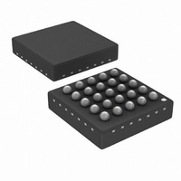
Connection Diagrams GR Package 3mm × 3mm × 1mm Top View Order Number LM49100GR See NS Package Number GRA25A GR Package Marking 300015f6 Top View XY — 2 Digit datecode TT — Lot traceability G — Boomer Family C9 — ...
Page 4
Bump Descriptions Bump Name Description Positive Charge Pump Power Supply DD A2 GNDCP Charge Pump Ground A3 MIN+ Positive Mono Input A4 BYPASS Half-Supply Bypass A5 RIN Right Input B1 C1N Negative Terminal – Charge Pump Flying ...
Page 5
... Absolute Maximum Ratings If Military/Aerospace specified devices are required, please contact the National Semiconductor Sales Office/ Distributors for availability and specifications. Supply Voltage (Loudspeaker) Supply Voltage (Headphone) Storage Temperature Input Voltage Power Dissipation (Note 3) ESD Susceptibility (Note 4) ESD Susceptibility (Note 5) Junction Temperature ...
Page 6
Symbol Parameter P Output Power OUT P Output Power OUT Total Harmonic Distortion + THD+N Noise Total Harmonic Distortion + THD+N Noise Total Harmonic Distortion + THD+N Noise www.national.com Conditions 1kHz 10% = 16Ω ...
Page 7
Symbol Parameter e Noise N T Turn-on Time ON T Turn-off Time OFF Z Input Impedance IN A Volume Control V CMRR Common Mode Rejection Ratio PSRR Power Supply Rejection Ratio PSRR Power Supply Rejection Ratio PSRR Power Supply Rejection ...
Page 8
(Notes 2, 7) The following specifications apply for V Symbol Parameter Clock Period Data Setup Time Data Stable Time Start Condition ...
Page 9
Typical Performance Characteristics THD+N vs Frequency = 8Ω 3.6V 22kHz, LS, Mode 1 THD+N vs Frequency = 8Ω 3V 215mW 22kHz, ...
Page 10
THD+N vs Frequency = 8Ω 5V 22kHz, Loudspeaker, Mode 1 THD+N vs Output Power = 32Ω 1kHz 22kHz, HP, Mode 4 Output Power vs Supply Voltage ...
Page 11
Power Dissipation vs Output Power = 8Ω 3.6V 1kHz, Mode 1 300015p5 Power Dissipation vs Output Power = 8Ω 5V 1kHz, Mode 1 300015p7 Supply Current ...
Page 12
PSRR vs Frequency = 32Ω 200mV L RIPPLE = 4.7μF, Mode 2, 10 2.8V PSRR vs Frequency = 32Ω 200mV L RIPPLE = 4.7μF, Mode 6, HP ...
Page 13
PSRR vs Frequency = 8Ω 200mV RIPPLE PP = 4.7μF, Mode 7, 10, 14, LS+ 2.8V PSRR vs Frequency = 8Ω 200mV ...
Page 14
LM49100 Control Tables The LM49100 is controlled through 1). D7 Modes Control 0 HP Volume (Gain) 0 Control Mono Volume 1 Control Left Volume (Gain) 1 Control Right Volume (Gain) 1 Control The following bits have added ...
Page 15
TABLE 4. Mono/Stereo Left/Stereo Right Input Gain Control Volume Step MV4/LV4/RV4 MV3/LV3/RV3 MV2/LV2/RV2 MV1/LV1/RV1 MV0/LV0/RV0 R/L Gain ...
Page 16
Application Information MINIMIZING CLICK AND POP To minimize the audible click and pop heard through a head- phone, maximize the input signal through the corresponding volume (gain) control registers and adjust the output amplifier gain accordingly to achieve the user’s ...
Page 17
PCB LAYOUT AND SUPPLY REGULATION CONSIDERATIONS FOR DRIVING 8Ω LOAD Power dissipated by a load is a function of the voltage swing across the load and the load's impedance. As load impedance decreases, load dissipation becomes increasingly dependent on the ...
Page 18
DMAX JMAX A The LM49100 150°C. In the GR package, the JMAX LM49100's θ is 50.2°C/W. At any given ambient tempera- JA ture T , use Equation (4) to find ...
Page 19
Demo Board Schematic 19 www.national.com ...
Page 20
Demonstration Board Layout www.national.com Signal 1 Layer Signal 2 Layer 20 300015f0 300015f1 ...
Page 21
Top Layer 300015f3 Top Overlay 21 www.national.com ...
Page 22
Bottom Layer Bottom Overlay 22 300015e8 300015e9 ...
Page 23
Revision History Rev Date 1.0 06/21/07 1.1 06/28/07 1.2 08/09/07 1.3 08/13/07 1.4 08/14/07 1.5 09/18/07 Description Initial release. Changed the mktg outline from TLA25XXX to GRA25A. Replaced some curves. Changed the f = 1kHz into f = 217Hz (PSRR) ...
Page 24
Physical Dimensions www.national.com inches (millimeters) unless otherwise noted Dimensions mm Package Order Number LM49100GR See NS Package Number GRA25A ...
Page 25
Notes 25 www.national.com ...
Page 26
... National Semiconductor and the National Semiconductor logo are registered trademarks of National Semiconductor Corporation. All other brand or product names may be trademarks or registered trademarks of their respective holders. ...