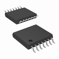
LM4854IBL/NOPB National Semiconductor, LM4854IBL/NOPB Datasheet - Page 22

LM4854IBL/NOPB
Manufacturer Part Number
LM4854IBL/NOPB
Description
IC AMP AUDIO PWR 2.3W AB 12USMD
Manufacturer
National Semiconductor
Series
Boomer®r
Type
Class ABr
Datasheet
1.LM4854MTXNOPB.pdf
(29 pages)
Specifications of LM4854IBL/NOPB
Output Type
1-Channel (Mono) with Stereo Headphones
Max Output Power X Channels @ Load
2.3W x 1 @ 3.2 Ohm; 200mW x 2 @ 16 Ohm
Voltage - Supply
2.4 V ~ 5.5 V
Features
Depop, Shutdown, Standby, Thermal Protection
Mounting Type
Surface Mount
Package / Case
12-MicroSMD
Lead Free Status / RoHS Status
Lead free / RoHS Compliant
Other names
LM4854IBL
LM4854IBLTR
LM4854IBLTR
www.national.com
Application Information
Figure 4 shows an optional resistor connected between the
amplifier output that drives the headphone jack sleeve and
ground. This resistor provides a ground path that supressed
power supply hum. This hum may occur in applications such
as notebook computers in a shutdown condition and con-
nected to an external powered speaker. The resistor’s 100Ω
value is a suggested starting point. Its final value must be
determined based on the tradeoff between the amount of
noise suppression that may be needed and minimizing the
additional current drawn by the resistor (25mA for a 100Ω
resistor and a 5V supply).
Single-Ended Output Power Performance and Measure-
ment Considerations
The LM4854 delivers clean, low distortion SE output power
into loads that are greater than 10Ω. As an example, output
power for 16Ω and 32Ω loads are shown in the Typical
Performance Characteristic curves. For loads less than 10Ω,
the LM4854 can typically supply 180mW of low distortion
power. However, when higher dissipation is desired in loads
less than 10Ω, a dramatic increase in THD+N may occur.
This is normal operation and does not indicate that proper
functionality has ceased. When a jump from moderate to
excessively high distortion is seen, simply reducing the out-
put voltage swing will restore the clean, low distortion SE
operation.
The dramatic jump in distortion for loads less than 10Ω
occurs when current limiting circuitry activates. During SE
operation, AMP2 (refer to Figure 2) drives the headphone
sleeve. An on-board circuit monitors this amplifier’s output
current. The sudden increase in THD+N is caused by the
current limit circuitry forcing AMP2 into a high-impedance
output mode. When this occurs, the output waveform has
discontinuities that produce large amounts of distortion. It
has been observed that as the output power is steadily
increased, the distortion may jump from 5% to greater than
35%. Indeed, 10% THD+N may not actually be achievable.
ESD Protection
As stated in the Absolute Maximum Ratings, the AMP2
output pin has a maximum ESD susceptibility rating of
8000V. For higher ESD voltages, the addition of a PCDN042
dual transil (from California Micro Devices), as shown in
Figure 4, will provide additional protection.
FIGURE 3. Headphone Circuit
(Continued)
20038212
22
SELECTING EXTERNAL COMPONENTS
Input Capacitor Value Selection
Amplifying the lowest audio frequencies requires high value
input coupling capacitor (Ci in Figure 2). A high value capaci-
tor can be expensive and may compromise space efficiency
in portable designs. In many cases, however, the speakers
used in portable systems, whether internal or external, have
little ability to reproduce signals below 150Hz. Applications
using speakers with this limited frequency response reap
little improvement by using large input capacitor.
The LM4854’s advanced output transient suppression cir-
cuitry has eliminated the need to select the input capacitor’s
value in relation to the BYPASS capacitor’s value as was
necessary in some previous Boomer amplifiers. The value of
CI is now strictly determined by the desired low frequency
response.
As shown in Figure 2, the input resistor (R
capacitor (C
is found using Equation (7).
As an example when using a speaker with a low frequency
limit of 150Hz, C
C
ciency, full range speaker whose response extends below
30Hz.
Bypass Capacitor Value Selection
Besides minimizing the input capacitor size, careful consid-
eration should be paid to value of CB, the capacitor con-
nected to the BYPASS pin. Since C
the LM4854 settles to quiescent operation, its value is critical
when minimizing turn-on pops. The slower the LM4854’s
outputs ramp to their quiescent DC voltage (nominally V
2), the smaller the turn-on pop. Choosing C
along with a small value of Ci (in the range of 0.1µF to
0.39µF), produces a click-less and pop-less shutdown func-
tion. As discussed above, choosing C
sary for the desired bandwidth helps minimize clicks and
pops. CB’s value should be in the range of 5 times to 7 times
the value of C
eliminated when power is first applied or the LM4854 re-
sumes operation after shutdown.
i
protection beyond the 8000V shown in the Absolute
shown in Figure 2 allows the LM4854 to drive high effi-
FIGURE 4. The PCDN042 provides additional ESD
Maximum Ratings for the AMP2 output
i
) produce a high pass filter cutoff frequency that
i
. This ensures that output transients are
i
, using Equation (7) is 0.063µF. The 1.0µF
f
c
= 1 / (2πR
i
C
i
)
B
i
no larger than neces-
determines how fast
200382E8
B
i
) and the input
equal to 1.0µF
DD
(7)
/


