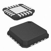
ISL54004IRTZ Intersil, ISL54004IRTZ Datasheet - Page 3

ISL54004IRTZ
Manufacturer Part Number
ISL54004IRTZ
Description
IC AMP AUDIO PWR 1.23W AB 20TQFN
Manufacturer
Intersil
Type
Class ABr
Datasheet
1.ISL54004IRTZ.pdf
(13 pages)
Specifications of ISL54004IRTZ
Output Type
1-Channel (Mono) with Stereo Headphones
Max Output Power X Channels @ Load
1.23W x 1 @ 8 Ohm; 215mW x 2 @ 16 Ohm
Voltage - Supply
2.7 V ~ 5.5 V
Features
Depop, Shutdown, Thermal Protection
Mounting Type
Surface Mount
Package / Case
20-TQFN
Lead Free Status / RoHS Status
Lead free / RoHS Compliant
Electrical Specifications - 5V Supply
Absolute Maximum Ratings
VDD to GND . . . . . . . . . . . . . . . . . . . . . . . . . . . . . . . -0.3V to +6.5V
Input Voltages
Output Voltages
Continuous Current (VDD, SPK_, Hp_, GND) . . . . . . . . . . . 750mA
ESD Rating
Operating Conditions
Temperature Range . . . . . . . . . . . . . . . . . . . . . . . . . -40°C to +85°C
CAUTION: Do not operate at or near the maximum ratings listed for extended periods of time. Exposure to such conditions may adversely impact product reliability and
result in failures not covered by warranty.
NOTE:
GENERAL
Power Supply Range, V
Quiescent Supply Current, I
Shutdown Supply Current, I
Input Resistance, R
Thermal Shutdown, T
Thermal Shutdown Hysteresis
SD to Full Operation, t
Gain Selection Range
BTL AMPLIFIER DRIVER, HD = V
Output Offset Voltage, V
Power Supply Rejection Ratio, PSRR V
Output Power, P
1. θ
2. For θ
InR, InL, SD, HD, HO, GSO, GS1. . . . . . . -0.3V to (VDD + 0.3V)
SPK+, SPK-, HpL, HpR . . . . . . . . . . . . . . -0.3V to (VDD + 0.3V)
Human Body Model . . . . . . . . . . . . . . . . . . . . . . . . . . . . . . . >2kV
Machine Model . . . . . . . . . . . . . . . . . . . . . . . . . . . . . . . . . >200kV
Charged Device Model . . . . . . . . . . . . . . . . . . . . . . . . . . . . . >1kV
Tech Brief TB379.
JA
is measured in free air with the component mounted on a high effective thermal conductivity test board with “direct attach” features. See
JC
PARAMETER
, the “case temp” location is the center of the exposed metal pad on the package underside.
OUT
IN
SD
SD(ON)
DD
OS
SD
DD
3
INH,
HO = V
coupled to GND (0.1µF)
SD = V
(BTL) and R
(0.1µF)
INS = 0V or V
INS = MIX = 0V or V
Input referred minimum gain
GS0 = GS1 = V
Input referred maximum gain
GS0 = GS1 = V
Input referred minimum gain
GS0 = GS1 = V
Input referred maximum gain
GS0 = GS1 = V
Measured between SPK+ and SPK-, Inputs AC
coupled to GND (0.1µF)
HD = V
coupled to GND (0.1µF)
R
R
RIPPLE
L
L
HO = V
= 8Ω, THD+N = 1%, f = 1kHz
= 8Ω, THD+N = 10%, f = 1kHz
INH
INL
INL
INH,
= 200MV
, HO = V
, RL = 8Ω, Inputs AC
or V
L
= 32Ω (SE), Inputs AC coupled to GND
DD
Test Conditions: V
C
GND for SE drivers, Unless Otherwise Specified (Note 3).
UNLESS OTHERWISE SPECIFIED
INH
REF
INL,
INH,
INL,
INH,
TEST CONDITIONS
, HD = V
P-P
INL
R
R
DD
= 1µF, R
R
R
,
L
L
L
L
or V
= 32Ω
= 8Ω
= 32Ω
= 8Ω
INL
INH
ISL54004
L
, R
, HD = V
is terminated between SPK+ and SPK- for BTL driver and between Hp_ and
L
DD
SE Amplifiers
HD = V
HO = V
BTL Amplifier
HD = V
HO = V
F
F
= None, Inputs AC
RIPPLE
RIPPLE
= +5V, GND = 0V, V
INL
Thermal Information
Thermal Resistance (Typical, Note 1, 2)
Maximum Junction Temperature . . . . . . . . . . . . . . . . . . . . . +150°C
Maximum Storage Temperature Range . . . . . . . . . . . -65°C to +150°C
Pb-free reflow profile . . . . . . . . . . . . . . . . . . . . . . . . . see link below
INH
INL
INH
INH
20 Ld 4x4 TQFN Package . . . . . . . . . .
http://www.intersil.com/pbfree/Pb-FreeReflow.asp
, R
= 217Hz
= 1kHz
L
= 8Ω
TEMP
(°C)
Full
Full
Full
Full
Full
25
25
25
25
25
25
25
25
25
25
25
25
25
25
INH
= 2.4V, V
(Notes 4, 5)
17.2
MIN
11.4
-0.4
2.7
5.2
-
-
-
-
-
-
-
-
-
-
-
-
-
-
INL
= 0.8V, SD = GSO = GS1 = V
TYP
1.23
100
150
941
4.6
5.5
28
31
10
12
18
38
49
49
47
1
0
6
-
θ
JA
(Notes 4, 5)
(°C/W)
45
MAX
12.6
18.6
5.5
0.6
6.6
12
50
-
-
-
-
-
-
-
-
-
-
-
-
October 30, 2007
θ
JC
UNITS
6.5
FN6513.2
(°C/W)
mW
mA
mA
mA
mA
mV
mV
ms
kΩ
dB
dB
dB
dB
dB
dB
°C
°C
W
V
INL
,


