2N2907A MICROSEMI, 2N2907A Datasheet - Page 4
2N2907A
Manufacturer Part Number
2N2907A
Description
Manufacturer
MICROSEMI
Datasheet
1.2N2907A.pdf
(6 pages)
Specifications of 2N2907A
Transistor Polarity
PNP
Number Of Elements
1
Collector-emitter Voltage
60V
Collector-base Voltage
60V
Emitter-base Voltage
5V
Collector Current (dc) (max)
600mA
Dc Current Gain (min)
100
Power Dissipation
400mW
Operating Temp Range
-65C to 200C
Operating Temperature Classification
Military
Mounting
Through Hole
Pin Count
3
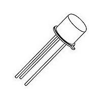
Package Type
TO-18
Lead Free Status / Rohs Status
Not Compliant
Available stocks
Company
Part Number
Manufacturer
Quantity
Price
Company:

Part Number:
2N2907A
Manufacturer:
VISHAY
Quantity:
4 500
Company:
Part Number:
2N2907A
Manufacturer:
MOT
Quantity:
1 746
Company:
Part Number:
2N2907A
Manufacturer:
MOT
Quantity:
3 077
Part Number:
2N2907A
Manufacturer:
MOC
Quantity:
20 000
Part Number:
2N2907AJAN
Manufacturer:
MOTOROLA/摩托罗拉
Quantity:
20 000
Part Number:
2N2907AUB
Manufacturer:
MICROSEMI/美高森美
Quantity:
20 000


6 Lake Street, Lawrence, MA 01841
1-800-446-1158 / (978) 620-2600 / Fax: (978) 689-0803
Website: http: //www.microsemi.com
NOTES:
1. Dimensions are in inches.
2. Millimeters are given for general information only.
3. Dimension “CH” controls the overall package thickness. When a
4. The corner shape (square, notch, radius) may vary at the
5. Dimensions “LW2” minimum and “L3” minimum and the appropriate
6. The co-planarity deviation of all terminal contact points, as defined
7. In accordance with ASME Y14.5M, diameters are equivalent to φx
T4-LDS-0059 Rev. 2 (100247)
.010 inch (0.254 mm) and a maximum of .040 inch (1.020 mm).
window lid is used, dimension “CH” must increase by a minimum of
manufacturer's option, from that shown on the drawing.
castellation length define an unobstructed three-dimensional space
traversing all of the ceramic layers in which a castellation was
designed. (Castellations are required on the bottom two layers,
optional on the top ceramic layer.) Dimension “LW2” maximum and
“L3” maximum define the maximum width and depth of the
castellation at any point on its surface. Measurement of these
dimensions may be made prior to solder dipping.
by the device seating plane, shall not exceed .006 inch (0.15mm) for
solder dipped leadless chip carriers.
symbology.
FIGURE 2. Physical dimensions, surface mount (UA version)
TECHNICAL DATA SHEET
Pin no.
Transistor
Symbol
BW2
LW2
BL2
LL1
LL2
BW
LW
CH
BL
LH
L3
LS
.145
.061
.003
.032
.072
.006
Min
.215
.029
.045
.022
Collector
Inches
1
Max
.225
.225
.155
.155
.075
.007
.042
.048
.088
.055
.028
.022
Dimensions
Emitter
2
5.46
3.68
1.55
0.08
0.74
0.81
1.83
1.14
0.56
0.15
Min
Millimeters
Base
Max
5.71
5.71
3.93
3.93
1.90
0.18
1.07
1.22
2.23
1.39
0.71
0.56
Page 4 of 6
3
Note
N/C
3
5
5
4
Related parts for 2N2907A
Image
Part Number
Description
Manufacturer
Datasheet
Request
R

Part Number:
Description:
MICROSEMI DIODE
Manufacturer:
MICROSEMI
Datasheet:

Part Number:
Description:
Schottky Rectifier
Manufacturer:
Microsemi Corporation
Datasheet:
Part Number:
Description:
Schottky Rectifier
Manufacturer:
Microsemi Corporation
Datasheet:
Part Number:
Description:
Schottky Rectifier
Manufacturer:
Microsemi Corporation
Datasheet:
Part Number:
Description:
Schottky Rectifier
Manufacturer:
Microsemi Corporation
Datasheet:
Part Number:
Description:
Ultra Fast Rectifier (less than 100ns)
Manufacturer:
Microsemi Corporation
Datasheet:
Part Number:
Description:
Manufacturer:
Microsemi Corporation
Datasheet:
Part Number:
Description:
Ultra Fast Rectifier (less than 100ns)
Manufacturer:
Microsemi Corporation
Datasheet:
Part Number:
Description:
Ultra Fast Rectifier (less than 100ns)
Manufacturer:
Microsemi Corporation
Datasheet:
Part Number:
Description:
Manufacturer:
Microsemi Corporation
Datasheet:
Part Number:
Description:
Manufacturer:
Microsemi Corporation
Datasheet:
Part Number:
Description:
Manufacturer:
Microsemi Corporation
Datasheet:
Part Number:
Description:
Manufacturer:
Microsemi Corporation
Datasheet:
Part Number:
Description:
Manufacturer:
Microsemi Corporation
Datasheet:
Part Number:
Description:
Manufacturer:
Microsemi Corporation
Datasheet: