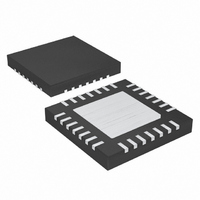
MAX9729ETI+ Maxim Integrated Products, MAX9729ETI+ Datasheet - Page 13

MAX9729ETI+
Manufacturer Part Number
MAX9729ETI+
Description
IC AMP AUDIO .052W STER 28TQFN
Manufacturer
Maxim Integrated Products
Series
DirectDrive™r
Type
Class ABr
Datasheet
1.MAX9729ETI.pdf
(28 pages)
Specifications of MAX9729ETI+
Output Type
Headphones, 2-Channel (Stereo)
Max Output Power X Channels @ Load
52mW x 2 @ 32 Ohm
Voltage - Supply
1.8 V ~ 3.6 V
Features
Bass Boost, Depop, I²C, Input Multiplexer, Short-Circuit and Thermal Protection, Shutdown, Volume Control
Mounting Type
Surface Mount
Package / Case
28-TQFN Exposed Pad
Product
General Purpose Audio Amplifiers
Output Power
49 mW
Thd Plus Noise
0.04 %
Supply Current
5.5 mA
Maximum Power Dissipation
2286 mW
Maximum Operating Temperature
+ 85 C
Mounting Style
SMD/SMT
Audio Load Resistance
16 Ohms
Minimum Operating Temperature
- 40 C
Amplifier Class
AB
No. Of Channels
2
Supply Voltage Range
1.8V To 3.6V
Load Impedance
32ohm
Operating Temperature Range
-40°C To +85°C
Amplifier Case Style
TQFN
Rohs Compliant
Yes
Lead Free Status / RoHS Status
Lead free / RoHS Compliant
The MAX9729 features a BEEP input with eight different
attenuation settings (see Table 6). The BEEP input is
useful for applications requiring the routing of a system
alert signal to the stereo audio path. The attenuation
value of the BEEP input is set by bits [7:5] in the 0x01
command register (see Tables 2 and 6). The attenua-
tion settings of the BEEP input are independent of the
volume settings stored in register 0x00 (see Table 2).
The BEEP input is enabled when BEEP_EN is connect-
ed to V
BEEP_EN is high, the selected INL_ and INR_ inputs
are disconnected from the signal path and the BEEP
input signal is routed to both headphone outputs after
being attenuated by the value set by bits [7:5] in regis-
ter 0x01. When BEEP_EN is low, the BEEP input is dis-
connected from the signal path and the selected INL_
and INR_ inputs are reconnected.
The MAX9729 includes a stereo 3:1 multiplexer/mixer,
allowing selection and mixing of three different stereo
input sources. Bits [6:5] in register 0x00 control the
selection/mixing of the input signal sources (see Tables
2 and 4). When all three stereo inputs are selected (Bits
[6:5] = 11), the stereo signals are summed (mixed)
together and connected to the signal path. The
MAX9729 implements the automatic volume ramping
function when an input source change occurs to ensure
smooth sounding transitions. Clipping may occur if
three high level signals are summed. Reprogram the
preamplifier maximum gain setting to compensate.
The MAX9729 features an I
serial interface consisting of a serial data line (SDA) and
Figure 3. 2-Wire Serial-Interface Timing Diagram
SDA
SCL
DD
t
HD, STA
Stereo Headphone Amplifier with BassMax,
and disabled when driven low. When
CONDITION
START
______________________________________________________________________________________
t
LOW
Input Multiplexer/Mixer
2
C/SMBus-compatible 2-wire
t
R
t
t
SU, DAT
HIGH
Serial Interface
t
F
BEEP Input
Volume Control, and Input Mux
t
HD, DAT
t
SU, STA
a serial clock line (SCL). SDA and SCL facilitate bidirec-
tional communication between the MAX9729 and the
master at clock rates up to 400kHz. Figure 3 shows the
2-wire interface timing diagram. The MAX9729 is a
transmit/receive slave-only device, relying upon a mas-
ter device to generate the clock signal. The master
device, typically a microcontroller, initiates data transfer
on the bus and generates SCL to permit that transfer.
A master device communicates to the MAX9729 by
transmitting the slave address with the Read/Write
(R/W) bit followed by the data word. Each transmit
sequence is framed by a START (S) or REPEATED
START (Sr) condition and a STOP (P) condition. Each
word transmitted over the bus is 8 bits long and is
always followed by an acknowledge or not acknowl-
edge clock pulse.
The MAX9729 SDA line operates as both an input and
an open-drain output. A pullup resistor, greater than
500Ω, is required on the SDA bus. The MAX9729 SCL
line operates as an input only. A pullup resistor, greater
than 500Ω, is required on SCL unless the MAX9729 is
operating in a single-master system where the master
device has a push-pull SCL output. Series resistors in
line with SDA and SCL are optional. Series resistors
protect the digital inputs of the MAX9729 from high-
voltage spikes on the bus lines, and minimize crosstalk
and undershoot of the bus signals.
One data bit is transferred during each SCL cycle. The
data on SDA must remain stable during the high period
of the SCL pulse since changes in SDA while SCL is
high are control signals (see the START and STOP
Conditions section). SDA and SCL idle high when the
I
CONDITION
REPEATED
2
START
C bus is not busy.
t
HD, STA
t
SP
t
SU, STO
CONDITION
STOP
t
BUF
CONDITION
Bit Transfer
START
13


