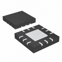
MAX9728AETC+ Maxim Integrated Products, MAX9728AETC+ Datasheet - Page 2

MAX9728AETC+
Manufacturer Part Number
MAX9728AETC+
Description
IC AMP AUDIO .06W STER AB 12TQFN
Manufacturer
Maxim Integrated Products
Series
DirectDrive™r
Type
Class ABr
Datasheet
1.MAX9728AETC.pdf
(19 pages)
Specifications of MAX9728AETC+
Output Type
Headphones, 2-Channel (Stereo)
Max Output Power X Channels @ Load
60mW x 2 @ 32 Ohm
Voltage - Supply
4.5 V ~ 5.5 V
Features
Depop, Short-Circuit and Thermal Protection, Shutdown
Mounting Type
Surface Mount
Package / Case
12-TQFN Exposed Pad
Product
General Purpose Audio Amplifiers
Output Power
60 mW
Thd Plus Noise
0.02 %
Operating Supply Voltage
4.5 V to 5.5 V
Supply Current
3.5 mA
Maximum Power Dissipation
1177 mW
Maximum Operating Temperature
+ 85 C
Mounting Style
SMD/SMT
Minimum Operating Temperature
- 40 C
Supply Voltage (max)
5.5 V
Supply Voltage (min)
4.5 V
Amplifier Class
AB
No. Of Channels
2
Supply Voltage Range
4.5V To 5.5V
Load Impedance
32ohm
Operating Temperature Range
-40°C To +85°C
Amplifier Case Style
TQFN
Rohs Compliant
Yes
Lead Free Status / RoHS Status
Lead free / RoHS Compliant
ABSOLUTE MAXIMUM RATINGS
V
PV
PGND to SGND .....................................................-0.3V to +0.3V
C1P to PGND..............................................-0.3V to (V
C1N to PGND............................................(PV
PV
IN_ to SGND (MAX9728A)..........................-0.3V to (V
IN_ to SGND (MAX9728B) .............(SV
OUT_ to SV
OUT_ to V
SHDN to _GND.........................................................-0.3V to +6V
ELECTRICAL CHARACTERISTICS
(V
(R
are at T
60mW, DirectDrive, Stereo Headphone
Amplifiers with Shutdown
Stresses beyond those listed under “Absolute Maximum Ratings” may cause permanent damage to the device. These are stress ratings only, and functional
operation of the device at these or any other conditions beyond those indicated in the operational sections of the specifications is not implied. Exposure to
absolute maximum rating conditions for extended periods may affect device reliability.
2
Note 1: OUTR and OUTL should be limited to no more than 9V above SV
Note 2: OUTR and OUTL should be limited to no more than 9V below V
GENERAL
Supply Voltage Range
Quiescent Current
Shutdown Current
Shutdown to Full Operation
Input Impedance
Output Offset Voltage
Power-Supply Rejection Ratio
Output Power
Voltage Gain
Channel-to-Channel Gain
Tracking
Total Harmonic Distortion Plus
Noise
DD
DD
IN
SS
SS
_______________________________________________________________________________________
to PGND............................................................-0.3V to +6V
= 20kΩ, R
to SV
and SV
= 5V, PGND = SGND, SHDN = 5V, C1 = C2 = 1µF, R
A
= +25°C, unless otherwise noted.) (Note 3)
DD
SS
PARAMETER
SS
SS
(Note 2) ......+0.3V to Max (SV
.........................................................-0.3V to +0.3V
(Note 1) ....-0.3V to Min (V
F
to PGND..........................................-6V to +0.3V
= 30kΩ); for MAX9728B gain = -1.5V/V (internally set), T
SS
SYMBOL
THD+N
I
PSRR
P
DD
SHDN
t
V
V
- 0.3V) to (V
I
SON
R
A
OUT
CC
DD
OS
IN
V
SS
- SV
SS
- V
- 0.3V) to +0.3V
SS
DD
SHDN = SGND = PGND
MAX9728B, measured at IN_
V
f = 1kHz, 100mV
f = 20kHz, 100mV
R
R
MAX9728B (Note 4)
MAX9728B
R
R
R
+ 0.3V, +9V)
DD
L
L
L
L
L
- 0.3V, -9V)
DD
DD
DD
= 32Ω, THD+N = 1%
= 16Ω, THD+N = 1%
= 1kΩ, V
= 32Ω, P
= 16Ω, P
= 4.5V to 5.5V
+ 0.3V)
+ 0.3V)
+ 0.3V)
L
OUT
OUT
OUT
= ∞, resistive load reference to ground; for MAX9728A gain = -1.5V/V
CONDITIONS
P-P
= 2V
= 50mW, f
= 35mW, f
P-P
OUT_ Short Circuit to SGND ......................................Continuous
Short Circuit between OUTL and OUTR ....................Continuous
Continuous Input Current into PV
Continuous Input Current (any other pin) .........................±20mA
Continuous Power Dissipation (T
Operating Temperature Range ...........................-40°C to +85°C
Storage Temperature Range .............................-65°C to +150°C
Junction Temperature ......................................................+150°C
Lead Temperature (soldering, 10s) .................................+300°C
12-Pin TQFN (derate 14.7mW/°C above +70°C) .........1177mW
14-Pin TSSOP (derate 9.1mW/°C above +70°C) ...........727mW
RMS
DD
SS
A
, or below SV
, f
= -40°C to +85°C, unless otherwise noted. Typical values
, or above V
IN
IN
IN
= 1kHz
= 1kHz
= 1kHz
DD
SS
- 0.3V, whichever limits first.
+ 0.3V, whichever limits first.
-1.52
MIN
4.5
15
30
A
SS
= +70°C)
..................................260mA
±0.15
< 0.1
0.003
±1.5
TYP
0.02
0.04
180
-1.5
3.5
19
86
80
65
63
42
-1.48
MAX
±10
5.5
5.5
25
1
UNITS
mW
mA
mV
V/V
kΩ
dB
µA
µs
%
%
V


