LM48820TM/NOPB National Semiconductor, LM48820TM/NOPB Datasheet - Page 6
LM48820TM/NOPB
Manufacturer Part Number
LM48820TM/NOPB
Description
IC AMP AUDIO PWR .095W AB 14USMD
Manufacturer
National Semiconductor
Series
Boomer®r
Type
Class ABr
Datasheet
1.LM48820TMNOPB.pdf
(16 pages)
Specifications of LM48820TM/NOPB
Output Type
Headphones, 2-Channel (Stereo)
Max Output Power X Channels @ Load
95mW x 2 @ 16 Ohm
Voltage - Supply
1.6 V ~ 4.5 V
Features
Depop, Shutdown, Thermal Protection
Mounting Type
Surface Mount
Package / Case
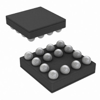
14-MicroSMD
Amplifier Class
AB
No. Of Channels
1
Output Power
95mW
Supply Voltage Range
1.6V To 4.5V
Load Impedance
2kohm
Operating Temperature Range
-40°C To +85°C
Amplifier Case Style
SMD
Rohs Compliant
Yes
For Use With
LM48820TMBD - BOARD EVAL GROUND REF AUDIO AMP
Lead Free Status / RoHS Status
Lead free / RoHS Compliant
Other names
LM48820TMTR


www.national.com
Z
I
L
Symbol
OUT
Note 1: All voltages are measured with respect to the GND pin unless otherwise specified.
Note 2: Absolute Maximum Ratings indicate limits beyond which damage to the device may occur. Operating Ratings indicate conditions for which the device is
functional but do not guarantee specific performance limits. Electrical Characteristics state DC and AC electrical specifications under particular test conditions
that guarantee specific performance limits. This assumes that the device is within the Operating Ratings. Specifications are not guaranteed for parameters where
no limit is given; however, the typical value is a good indication of device performance.
Note 3: The maximum power dissipation must be derated at elevated temperatures and is dictated by T
allowable power dissipation is P
for more information
Note 4: Human body model, 100pF discharged through a 1.5kΩ resistor.
Note 5: Machine Model, 220pF - 240pF discharged through all pins.
Note 6: Typicals are measured at 25°C and represent the parametric norm.
Note 7: Limits are guaranteed to National's AOQL (Average Outgoing Quality Level).
Note 8: Datasheet min/max specification limits are guaranteed by design, test, or statistical analysis.
Note 9: θ
Note 10: V
External Components Description
(Figure 1)
Components
1.
3.
4.
5.
2
JA
C
OUT
value is measured with the device mounted on a PCB with a 3” x 1.5”, 1oz copper heatsink.
INR/INL
Output Impedance
Input Leakage
C
C
C
C
SS
S1
S2
refers to signal applied to the LM48820 outputs.
C
Input coupling capacitor which blocks the DC voltage at the amplifier's input terminals. Also creates a high-pass
filter with R
of how to determine the value of C
Flying capacitor. Low ESR ceramic capacitor (
Output capacitor. Low ESR ceramic capacitor (
Tantalum capacitor. Supply bypass capacitor which provides power supply filtering. Refer to the Power Supply
Bypassing section for information concerning proper placement and selection of the supply bypass capacitor.
Ceramic capacitor. Supply bypass capacitor which provides power supply filtering. Refer to the Power Supply
Bypassing section for information concerning proper placement and selection of the supply bypass capacitor.
Parameter
DMAX
i
at f
= (T
C
JMAX
= 1/(2πR
- T
A
) / θ
i
C
JA
IN
SD_LC = SD_RC = GND
–500mV
(Note 10)
or the number given in Absolute Maximum Ratings, whichever is lower. See power dissipation curves
). Refer to the section Proper Selection of External Components, for an explanation
i
.
≤
V
OUT
Conditions
Functional Description
≤
6
≤
V
≤
100mΩ)
DD
100mΩ)
+500mV
JMAX
, θ
JA
, and the ambient temperature, T
(Note 6)
Typical
±0.1
8
LM48820
(Notes 7, 8)
Limit
2
A
. The maximum
kΩ (min)
(Limits)
Units
nA
Related parts for LM48820TM/NOPB
Image
Part Number
Description
Manufacturer
Datasheet
Request
R

Part Number:
Description:
IC,Audio Amplifier,DUAL,BGA,14PIN,PLASTIC
Manufacturer:
National Semiconductor
Part Number:
Description:
250mW Audio Power Amplifier with Shutdown Mode
Manufacturer:
National Semiconductor
Datasheet:
Part Number:
Description:
National Semiconductor [8-Bit D/A Converter]
Manufacturer:
National Semiconductor
Datasheet:
Part Number:
Description:
National Semiconductor [Media Coprocessor]
Manufacturer:
National Semiconductor
Datasheet:
Part Number:
Description:
Digitally Controlled Tone and Volume Circuit with Stereo Audio Power Amplifier, Microphone Preamp Stage and National 3D Sound
Manufacturer:
National Semiconductor
Datasheet:
Part Number:
Description:
Digitally Controlled Tone and Volume Circuit with Stereo Audio Power Amplifier, Microphone Preamp Stage and National 3D Sound
Manufacturer:
National Semiconductor
Datasheet:
Part Number:
Description:
AC97 Rev 2 Codec with Sample Rate Conversion and National 3D Sound
Manufacturer:
National Semiconductor
Part Number:
Description:
Manufacturer:
National Semiconductor
Datasheet:
Part Number:
Description:
Manufacturer:
National Semiconductor
Datasheet:
Part Number:
Description:
General Purpose, Low Voltage, Low Power, Rail-to-Rail Output Operational Amplifiers
Manufacturer:
National Semiconductor
Datasheet:
Part Number:
Description:
8-bit 20 MSPS flash A/D converter.
Manufacturer:
National Semiconductor
Datasheet:
Part Number:
Description:
Low Noise Quad Operational Amplifier
Manufacturer:
National Semiconductor
Datasheet:
Part Number:
Description:
Quad Differential Line Receivers
Manufacturer:
National Semiconductor
Datasheet:
Part Number:
Description:
Quad High Speed Trapezoidal? Bus Transceiver
Manufacturer:
National Semiconductor
Datasheet: