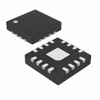
MAX9759ETE+ Maxim Integrated Products, MAX9759ETE+ Datasheet - Page 14

MAX9759ETE+
Manufacturer Part Number
MAX9759ETE+
Description
IC AMP AUDIO PWR 3.2W D 16TQFN
Manufacturer
Maxim Integrated Products
Type
Class Dr
Datasheet
1.MAX9759ETE.pdf
(20 pages)
Specifications of MAX9759ETE+
Output Type
1-Channel (Mono)
Max Output Power X Channels @ Load
4.3W x 1 @ 3 Ohm
Voltage - Supply
3 V ~ 5.5 V
Features
Depop, Differential Inputs, Mute, Short-Circuit and Thermal Protection, Shutdown
Mounting Type
Surface Mount
Package / Case
16-TQFN Exposed Pad
Product
Class-D
Output Power
3.2 W
Common Mode Rejection Ratio (min)
67 dB
Thd Plus Noise
0.03 %
Operating Supply Voltage
3 V to 5.5 V
Supply Current
8.4 mA
Maximum Power Dissipation
1.8 W
Maximum Operating Temperature
+ 85 C
Mounting Style
SMD/SMT
Minimum Operating Temperature
- 40 C
Supply Voltage (max)
5.5 V
Supply Voltage (min)
3 V
Amplifier Class
D
No. Of Channels
1
Supply Voltage Range
3V To 5.5V
Load Impedance
4ohm
Operating Temperature Range
-40°C To +85°C
Amplifier Case Style
TQFN
Rohs Compliant
Yes
Lead Free Status / RoHS Status
Lead free / RoHS Compliant
3.2W, High-Efficiency, Low-EMI,
Filterless, Class D Audio Amplifier
The MAX9759 features a mute function that disables
the H-bridge outputs of the switching amplifier. The
mute function only affects the power amplifiers of the
MAX9759; it does not shut down the device. Driving
MUTE low places the MAX9759 in a disabled output
mode. Drive MUTE high for normal operation.
The MAX9759 features comprehensive click-and-pop
suppression that eliminates audible transients on startup
and shutdown. While in shutdown, the H-bridge is in a
high-impedance state. During startup or power-up, the
input amplifiers are muted and an internal loop sets the
modulator bias voltages to the correct levels, preventing
clicks and pops when the H-bridge is subsequently
enabled. For 40ms following startup, a soft-start function
gradually unmutes the input amplifiers.
For improved click-and-pop performance, sequence the
digital inputs of the SHDN and MUTE pins of the
MAX9759 during power-up and power-down of the
device such that transients are eliminated from each
power cycle. Apply power to the MAX9759 with both
SHDN and MUTE held low. Release SHDN before MUTE
such that minimal transients occur during startup of the
device. The mute function allows the MAX9759 to be
powered up with the H-bridge outputs of the switching
amplifier disabled. For power-down, sequence the power
cycle such that the amplifier is muted first and subse-
quently shut down before power is disconnected from the
IC. This power cycle eliminates any audible transients on
power-up and power-down of the MAX9759.
Traditional Class D amplifiers require an output filter to
recover the audio signal from the amplifier’s output. The
filters add cost, increase the solution size of the amplifi-
er, and can decrease efficiency. The traditional PWM
scheme uses large differential output swings (2 x V
peak-to-peak) and causes large ripple currents. Any
parasitic resistance in the filter components results in a
loss of power, lowering the efficiency.
The MAX9759 does not require an output filter for the short
speaker cable. The device relies on the inherent induc-
tance of the speaker coil and the natural filtering of both
the speaker and the human ear to recover the audio com-
ponent of the square-wave output. Eliminating the output
filter results in a smaller, less costly, more efficient solution.
Because the frequency of the MAX9759 output is well
beyond the bandwidth of most speakers, voice coil
movement due to the switching frequency is very small.
14
______________________________________________________________________________________
Applications Information
Click-and-Pop Suppression
Filterless Operation
Mute
DD
Although this movement is small, a speaker not
designed to handle the additional power can be dam-
aged. For optimum results, use a speaker with a series
inductance > 10µH to 100µH range.
Unlike a Class AB amplifier, the output offset voltage of a
Class D amplifier does not noticeably increase quiescent
current draw when a load is applied. This is due to the
power conversion of the Class D amplifier. For example,
an 8mV DC offset across an 8Ω load results in 1mA extra
current consumption in a Class AB device. In the Class
D case, an 8mV offset into an 8Ω load equates to an
additional power drain of 8µW. Due to the high efficiency
of the Class D amplifier, this represents an additional
quiescent current draw of 8µW/(V
the order of a few microamps.
The MAX9759 features a differential input structure,
making it compatible with many CODECs, and offers
improved noise immunity over a single-ended input
amplifier. High-frequency signals can be picked up by
the amplifier’s input traces and can appear at the
amplifier’s inputs as common-mode noise. A differential
input amplifier amplifies the difference of the two
inputs; any signal common to both inputs is cancelled.
The MAX9759 can be configured as a single-ended input
amplifier by capacitively coupling one input to GND while
simultaneously driving the other input (Figure 6).
The input amplifier can accept DC-coupled inputs that
are biased within the amplifier’s common-mode range
(see the Typical Operating Characteristics). DC coupling
eliminates the input-coupling capacitors, reducing com-
ponent count to potentially one external component (see
the System Diagram). However, the low-frequency rejec-
tion of the capacitors is lost, allowing low-frequency sig-
nals to feedthrough to the load.
Figure 6. Single-Ended Input
SINGLE-ENDED
AUDIO INPUT
1µF
Power-Conversion Efficiency
1µF
IN+
IN-
MAX9759
DD
Single-Ended Input
/100η), which is on
Input Amplifier
DC-Coupled Input
Differential Input


