LMV1012UP-25/NOPB National Semiconductor, LMV1012UP-25/NOPB Datasheet
LMV1012UP-25/NOPB
Specifications of LMV1012UP-25/NOPB
LMV1012UP-25TR


Related parts for LMV1012UP-25/NOPB


LMV1012UP-25/NOPB Summary of contents
Page 1
... SMD packages. The LMV1012XP is designed for 1.0 mm canisters and thicker ECM canisters. These extremely miniature packages are designed for electret con- denser microphones (ECM) form factor. Schematic Diagram © 2005 National Semiconductor Corporation Features (Typical LMV1012-15, 2.2V supply unless otherwise specified) ...
Page 2
... Absolute Maximum Ratings If Military/Aerospace specified devices are required, please contact the National Semiconductor Sales Office/ Distributors for availability and specifications. ESD Tolerance (Note 2) Human Body Model Machine Model Supply Voltage V - GND DD 2.2V Electrical Characteristics Unless otherwise specified, all limits guaranteed for T Boldface limits apply at the temperature extremes ...
Page 3
Electrical Characteristics Unless otherwise specified, all limits guaranteed for T Boldface limits apply at the temperature extremes. Symbol Parameter A Gain V 5V Electrical Characteristics Unless otherwise specified, all limits guaranteed for T Boldface limits apply at the temperature ...
Page 4
Electrical Characteristics Unless otherwise specified, all limits guaranteed for T Boldface limits apply at the temperature extremes. Symbol Parameter C Input Capacitance IN Z Input Impedance IN A Gain V Note 1: Absolute Maximum Ratings indicate limits beyond which ...
Page 5
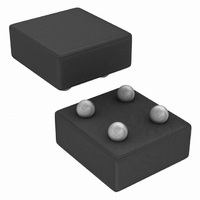
... LMV1012XP-25 lead free only LMV1012XPX-25 LMV1012UP-07 LMV1012UPX-07 LMV1012UP-15 4-Bump Ultra-Thin LMV1012UPX-15 micro SMD (0.4 mm max height) LMV1012UP-20 lead free only LMV1012UPX-20 LMV1012UP-25 LMV1012UPX-25 LMV1012TP-07 LMV1012TPX-07 4-Bump Thin LMV1012TP-15 micro SMD (0.5 mm max height) LMV1012TPX-15 lead free only LMV1012TP-25 LMV1012TPX-25 ...
Page 6
Typical Performance Characteristics C = 2.2 µF, single supply 25˚C A Supply Current vs. Supply Voltage (LMV1012-07) Supply Current vs. Supply Voltage (LMV1012-20) Gain and Phase vs. Frequency (LMV1012-07) www.national.com Unless otherwise specified, V Supply Current vs. Supply ...
Page 7
Typical Performance Characteristics C = 2.2 µF, single supply 25˚C (Continued) A Gain and Phase vs. Frequency (LMV1012-20) Total Harmonic Distortion vs. Frequency (LMV1012-07) Total Harmonic Distortion vs. Frequency (LMV1012-20) Unless otherwise specified, V Gain and Phase vs. ...
Page 8
Typical Performance Characteristics C = 2.2 µF, single supply 25˚C (Continued) A Total Harmonic Distortion vs. Input Voltage (LMV1012-07) Total Harmonic Distortion vs. Input Voltage (LMV1012-20) Output Noise vs. Frequency (LMV1012-07) www.national.com Unless otherwise specified, V Total Harmonic ...
Page 9
Typical Performance Characteristics C = 2.2 µF, single supply 25˚C (Continued) A Output Noise vs. Frequency (LMV1012-20) Unless otherwise specified, V Output Noise vs. Frequency (LMV1012-25) 20058728 9 = 2.2V 2.2 kΩ 20058716 www.national.com ...
Page 10
Application Section HIGH GAIN The LMV1012 series provides outstanding gain versus the JFET and still maintains the same ease of implementation, with improved gain, linearity and temperature stability. A high gain eliminates the need for extra external components. BUILT IN ...
Page 11
Application Section (Continued) SPL needs to be converted to the absolute sound pressure in dBPa. This is the sound pressure level in decibels referred to 1 Pascal (Pa). The conversion is given by: dBPa = dB SPL + 20*log 20 ...
Page 12
Application Section (Continued) www.national.com FIGURE 6. RF Noise Reduction 12 20058708 ...
Page 13
... Physical Dimensions inches (millimeters) unless otherwise noted NOTE: UNLESS OTHERWISE SPECIFIED. 1. FOR SOLDER BUMP COMPOSITION, SEE "SOLDER INFORMATION" IN THE PACKAGING SECTION OF THE NATIONAL SEMICONDUCTOR WEB PAGE (www.national.com). 2. RECOMMEND NON-SOLDER MASK DEFINED LANDING PAD. 3. PIN A1 IS ESTABLISHED BY LOWER LEFT CORNER WITH RESPECT TO TEXT ORIENTATION. ...
Page 14
... Physical Dimensions NOTE: UNLESS OTHERWISE SPECIFIED. 1. FOR SOLDER BUMP COMPOSITION, SEE "SOLDER INFORMATION" IN THE PACKAGING SECTION OF THE NATIONAL SEMICONDUCTOR WEB PAGE (www.national.com). 2. RECOMMEND NON-SOLDER MASK DEFINED LANDING PAD. 3. PIN A1 IS ESTABLISHED BY LOWER LEFT CORNER WITH RESPECT TO TEXT ORIENTATION. 4. XXX IN DRAWING NUMBER REPRESENTS PACKAGE SIZE VARIATION WHERE X1 IS PACKAGE WIDTH PACKAGE LENGTH AND X3 IS PACKAGE HEIGHT ...
Page 15
... BANNED SUBSTANCE COMPLIANCE National Semiconductor manufactures products and uses packing materials that meet the provisions of the Customer Products Stewardship Specification (CSP-9-111C2) and the Banned Substances and Materials of Interest Specification (CSP-9-111S2) and contain no ‘‘Banned Substances’’ as defined in CSP-9-111S2. ...