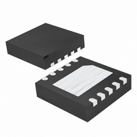
MAX9718AETB+T Maxim Integrated Products, MAX9718AETB+T Datasheet - Page 4

MAX9718AETB+T
Manufacturer Part Number
MAX9718AETB+T
Description
IC AMP AUDIO PWR 1.4W AB 10TDFN
Manufacturer
Maxim Integrated Products
Type
Class ABr
Datasheet
1.MAX9718AETBT.pdf
(27 pages)
Specifications of MAX9718AETB+T
Output Type
1-Channel (Mono)
Max Output Power X Channels @ Load
1.4W x 1 @ 4 Ohm
Voltage - Supply
2.7 V ~ 5.5 V
Features
Depop, Differential Inputs, Shutdown, Thermal Protection
Mounting Type
Surface Mount
Package / Case
10-TDFN Exposed Pad
Product
General Purpose Audio Amplifiers
Output Power
1.4 W
Common Mode Rejection Ratio (min)
- 60 dB
Thd Plus Noise
0.002 %
Supply Current
5 mA
Maximum Power Dissipation
1951 mW
Maximum Operating Temperature
+ 85 C
Mounting Style
SMD/SMT
Audio Load Resistance
4 Ohms
Minimum Operating Temperature
- 40 C
Amplifier Class
AB
No. Of Channels
1
Supply Voltage Range
2.7V To 5.5V
Load Impedance
4ohm
Operating Temperature Range
-40°C To +85°C
Amplifier Case Style
TDFN
Rohs Compliant
Yes
Lead Free Status / RoHS Status
Lead free / RoHS Compliant
Other names
MAX9718AETB+T
MAX9718AETB+TTR
MAX9718AETB+TTR
ELECTRICAL CHARACTERISTICS—3V Supply (continued)
(V
T
Low-Cost, Mono/Stereo,
1.4W Differential Audio Power Amplifiers
4
Note 1: All specifications are 100% tested at T
Note 2: Quiescent power-supply current is specified and tested with no load. Quiescent power-supply current depends on the offset
Note 3: Common-mode bias voltage is the voltage on BIAS and is nominally V
Note 4: Output power is specified by a combination of a functional output current test and characterization analysis.
Note 5: Measurement bandwidth for THD+N is 22Hz to 22kHz.
Note 6: Peak voltage measured at power-on, power-off, into or out of SHDN. Bandwidth defined by A-weighted filters, inputs at AC
(V
A
Output Power
Total Harmonic Distortion Plus
Noise
Thermal-Shutdown Threshold
Thermal-Shutdown Hysteresis
Maximum Capacitive Drive
Power-Up/Enable from
Shutdown Time
Shutdown Time
Turn-Off Transient
Crosstalk
CC
0.0001
CC
= +25°C. C
0.001
0.01
_______________________________________________________________________________________
0.1
10
= 3V, GND = 0, SHDN/SHDN = V
= 5V, C
1
TOTAL HARMONIC DISTORTION PLUS NOISE
10
design, not production tested.
voltage when a practical load is connected to the amplifier. Guaranteed by design.
GND. V
PARAMETER
V
R
A
CC
L
V
= 4Ω
= 2
= 5V
BIAS
BIAS
OUTPUT POWER = 50mW
100
CC
vs. FREQUENCY
= 0.1μF, THD+N measurement bandwidth = 22Hz to 22kHz, T
FREQUENCY (Hz)
= 0.1μF, no load. Typical values are at T
OUTPUT POWER = 1W
rise and fall times greater than or equal to 1ms.
1k
10k
SYMBOL
THD+N
C
t
P
V
SHDN
LOAD
t
OUT
POP
PU
100k
CC
(MAX9718/MAX9719), SHDM = GND (MAX9718), R
R
R
A
Bridge-tied capacitance
(Note 6)
MAX9719, f
0.0001
A
L
L
V
0.001
0.01
= +25°C. Specifications over temperature (T
= 8Ω, THD+N = 1%, f
= 8Ω, f
= 6dB
0.1
10
1
TOTAL HARMONIC DISTORTION PLUS NOISE
10
V
R
A
CC
L
V
IN
= 4Ω
= 4
IN
= 5V
= 1kHz, P
OUTPUT POWER = 200mW
A
= 1kHz
100
= +25°C, unless otherwise noted.) (Note 1)
CONDITIONS
vs. FREQUENCY
OUTPUT POWER = 1W
FREQUENCY (Hz)
OUT
1k
IN
Typical Operating Characteristics
= 0.25W,
= 1kHz (Note 4)
10k
CC
A
/2.
= +25°C, unless otherwise noted.)
100k
0.0001
0.001
0.01
A
0.1
10
1
= T
TOTAL HARMONIC DISTORTION PLUS NOISE
10
MIN
MIN
V
R
A
IN
CC
L
V
= 8Ω
= 2
= 5V
= R
to T
OUTPUT POWER = 250mW
100
OUTPUT POWER = 750mW
MAX
0.003
F
+160
TYP
vs. FREQUENCY
475
500
-85
15
10
40
FREQUENCY (Hz)
= 10kΩ (MAX971_A/H),
3
) are guaranteed by
1k
MAX
10k
UNITS
mW
mV
ms
dB
pF
°C
°C
μs
100k
%


