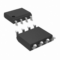
LM4876M/NOPB National Semiconductor, LM4876M/NOPB Datasheet - Page 10

LM4876M/NOPB
Manufacturer Part Number
LM4876M/NOPB
Description
IC AMP AUDIO PWR 1.5W MONO 8SOIC
Manufacturer
National Semiconductor
Series
Boomer®r
Type
Class ABr
Datasheet
1.LM4876MMNOPB.pdf
(12 pages)
Specifications of LM4876M/NOPB
Output Type
1-Channel (Mono)
Max Output Power X Channels @ Load
1.5W x 1 @ 8 Ohm
Voltage - Supply
2 V ~ 5.5 V
Features
Shutdown, Thermal Protection
Mounting Type
Surface Mount
Package / Case
8-SOIC (3.9mm Width)
Amplifier Class
AB
No. Of Channels
1
Output Power
1.1W
Supply Voltage Range
2V To 5.5V
Load Impedance
8ohm
Operating Temperature Range
-40°C To +85°C
Amplifier Case Style
SOIC
Rohs Compliant
Yes
Lead Free Status / RoHS Status
Lead free / RoHS Compliant
Other names
*LM4876M
*LM4876M/NOPB
LM4876M
*LM4876M/NOPB
LM4876M
www.national.com
Application Information
AUDIO POWER AMPLIFIER DESIGN
Audio Amplifier Design: Driving 1W into an 8Ω Load
The following are the desired operational parameters:
The design begins by specifying the minimum supply voltage
necessary to obtain the specified output power. One way to
find the minimum supply voltage is to use the Output Power
vs Supply Voltage curve in the Typical Performance Char-
acteristics section. Another way, using Equation (8), is to
calculate the peak output voltage necessary to achieve the
desired output power for a given load impedance. To ac-
count for the amplifier’s dropout voltage, two additional volt-
ages, based on the Dropout Voltage vs Supply Voltage in the
Typical Performance Characteristics curves, must be
added to the result obtained by Equation (8). This results in
Equation (9).
The Output Power vs Supply Voltage graph for an 8Ω load
indicates a minimum supply voltage of 4.6V. This is easily
met by the commonly used 5V supply voltage. The additional
voltage creates the benefit of headroom, allowing the
LM4876 to produce peak output power in excess of 1W
without clipping or other audible distortion. The choice of
supply voltage must also not create a violation of maximum
power dissipation as explained above in the Power Dissi-
pation section.
After satisfying the LM4876’s power dissipation require-
ments, the minimum differential gain is found using Equation
(10).
Power Output
Load Impedance
Input Level
Input Impedance
Bandwidth
V
CC
≥ (V
OUTPEAK
+ (V
100Hz–20kHz
OD TOP
+ V
(Continued)
OD BOT
±
))
1W
0.25dB
1V
20kΩ
RMS
RMS
8Ω
(8)
(9)
10
Thus, a minimum gain of 2.83 allows the LM4876’s to reach
full output swing and maintain low noise and THD+N perfor-
mance. For this example, let A
The amplifier’s overall gain is set using the input (R
feedback (R
set at 20kΩ, the feedback resistor is found using Equation
(11).
The value of R
The last step in this design example is setting the amplifier’s
-3dB low frequency bandwidth. To achieve the desired
±
quency response must extend to at least one-fifth the lower
bandwidth limit and the high frequency response must ex-
tend to at least five times the upper bandwidth limit. The
results is an
and an
As mentioned in the External Components section, R
create a highpass filter that sets the amplifier’s lower band-
pass frequency limit. Find the coupling capacitor’s value
using Equation (12).
The result is
Use a 0.39µF capacitor, the closest standard value.
The product of the desired high frequency cutoff (100kHz in
this example) and the differential gain, A
upper passband response limit. With A
100kHz, the closed-loop gain bandwidth product (GBWP) is
150kHz. This is less than the LM4876’s 4MHz GBWP. With
this margin, the amplifier can be used in designs that require
more differential gain and avoid performance-restricting
bandwidth limitations.
0.25dB pass band magnitude variation limit, the low fre-
f
F
L
1/(2π*20kΩ*20Hz) = 0.398µF.
H
= 100 Hz/5 = 20Hz
= 20 kHz*5 = 100kHz
f
) resistors. With the desired input impedance
f
is 30kΩ.
Ci ≥ 1/(2πRif
R
f
/R
i
VD
= A
= 3.
VD
/2
L
)
VD
VD
, determines the
= 3 and f
i
and C
i
) and
(10)
(12)
(11)
H
=
i


