NS16C2552TVA/NOPB National Semiconductor, NS16C2552TVA/NOPB Datasheet
NS16C2552TVA/NOPB
Specifications of NS16C2552TVA/NOPB
Available stocks


Related parts for NS16C2552TVA/NOPB

NS16C2552TVA/NOPB Summary of contents
Page 1
... The NS16C2552 and NS16C2752 have complete MODEM-con- trol capability, and a processor-interrupt system. The inter- rupts can be programmed by the user to minimize the processing required to handle the communications link. © 2009 National Semiconductor Corporation NS16C2552/NS16C2752 2.0 Features ■ Dual independent UART ■ ...
Page 2
General Description ......................................................................................................................... 1 2.0 Features ........................................................................................................................................ 1 3.0 System Block Diagram ..................................................................................................................... 4 4.0 Connection Diagrams ....................................................................................................................... 4 5.0 Pin Descriptions .............................................................................................................................. 5 5.1 PARALLEL BUS INTERFACE .................................................................................................... 5 5.2 SERIAL IO INTERFACE ........................................................................................................... 6 5.3 CLOCK AND ...
Page 3
Physical Dimensions .................................................................................................................... 43 FIGURE 1. Internal Clock Dividers ............................................................................................................... 18 FIGURE 2. Crystal Oscillator Circuitry .......................................................................................................... 26 FIGURE 3. Clock Input Circuitry .................................................................................................................. 27 FIGURE 4. Rx FIFO Mode ........................................................................................................................ 27 FIGURE 5. RXRDY in DMA Mode 1 ...
Page 4
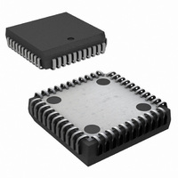
System Block Diagram 4.0 Connection Diagrams 44–PLCC Order Number NS16C2552TVA, NS16C2752TVA; See NS Package Number V44A www.national.com 20204802 48–TQFP Order Number NS16C2552TVS, NS16C2752TVS; See NS Package Number VBC48A 4 20204801 20204830 ...
Page 5
Pin Descriptions The NS16C2552/NS16C2752 pins are classified into the fol- lowing interface categories. • Bus Interface • Serial I/O Interface • Clock and Reset • Power supply and Ground pins Serial channel number ( designated by ...
Page 6
Signal PLCC TQFP Type Name Pin # Pin # TXRDY1 TXRDY2 32 28 INTR1 INTR2 17 12 5.2 SERIAL IO INTERFACE Signal PLCC TQFP Type Name Pin # Pin # SOUT1 ...
Page 7
Signal PLCC TQFP Type Name Pin # Pin # DCD1 DCD2 30 26 RI1 RI2 31 27 MF1 MF2 19 14 UART Data-carrier-detect: When low, DCD indicates that the data carrier ...
Page 8
CLOCK AND RESET Signal Type PLCC Name Pin # XIN I 11 XOUT 5.4 POWER AND GROUND Signal PLCC Type Name Pin # VCC GND N/A ...
Page 9
Register Set There are two identical register sets, one for each channel, in the DUART. All register descriptions in this section apply to the register sets in both channels. To clarify the descriptions of transmission and receiving op- erations, ...
Page 10
Reg RD/ Addr BIT 7 BIT 6 WR A2-A0 UART 16C550 Compatible Registers (Default Values Upon Reset) RBR R/W Data7 Data6 THR 0x0 Default X X IER R/W CTS Int RTS Int 0x1 Ena Ena Default 0 0 IIR R ...
Page 11
Reg RD/ Addr BIT 7 BIT 6 WR A2-A0 DLL R/W DLL DLL 0x0 Bit 7 Bit 6 Default X X DLM R/W DLM DLM 0x1 Bit 7 Bit 6 Default X X AFR R/W Rsrvd Rsrvd Rsrvd 0x2 Bit ...
Page 12
TRANSMIT HOLDING REGISTER (THR) This register holds the byte-wide transmit data (THR). This is a write-only register. Bit Bit Name 7:0 THR Data 6.3 INTERRUPT ENABLE REGISTER (IER) This register enables eight types of interrupts for the corre- sponding ...
Page 13
R/W Bit Bit Name Def 7:6 FIFOs Ena INT Src INT Src 3:1 INT Src 3:1 R 000 0 INT Src IIR Register Status Bits Priority Level ...
Page 14
Mode 0: Mode 0 allows for single transfer in each DMA cycle. When in the 16450 Mode (FCR[ the FIFO Mode (FCR[ FCR[ and there is at least one character in the ...
Page 15
R/W Bit Bit Name Def 1 Rx FIFO W Receive FIFO Reset Reset 0 This bit is only active when FCR bit Reset RCVR FIFO pointers and all bytes in the RCVR FIFO (the Rx ...
Page 16
LINE CONTROL REGISTER (LCR) The system programmer specifies the format of the asyn- chronous data communications exchange and sets the Divi- Bit Name R/W Bit Default Def 7 Divisor Latch R/W Ena Break Ena R/W 0 ...
Page 17
Bit Name R/W Bit Default Def 1:0 Tx/Rx Word R/W Tx and Rx Word Length Select Length Sel 0 These two bits specify the word length to be transmitted or received. LCR[ Description LCR[0] Word Length ...
Page 18
MODEM CONTROL REGISTER (MCR) This register controls the interface with the MODEM or data set (or a peripheral device emulating a MODEM). There is a clock divider for each channel. Each is capable of taking a R/W Bit Bit ...
Page 19
R/W Bit Bit Name Def 4 Internal R/W Internal Loopback Enable Loopback 0 This bit provides a local loopback feature for diagnostic testing of the associated serial channel. Ena (Refer to Section 7.8 INTERNAL LOOPBACK MODE and Figure 13.) 1 ...
Page 20
LINE STATUS REGISTER (LSR) This register provides status information to the CPU concern- ing the data transfer. R/W Bit Bit Name Def 7 Rx FIFO Err R Rx FIFO Data Error 0 This bit is a global Rx FIFO ...
Page 21
R/W Bit Bit Name Def 2 Rx Parity Error R Parity Error Indicator 0 This bit is the Parity Error (PE) indicator Received data word does not have the correct even or odd parity, as selected by the ...
Page 22
MODEM STATUS REGISTER (MSR) This register provides the current state of the control lines from the MODEM (or peripheral device) to the CPU. In addi- tion to this current-state information, four bits of the MODEM R/W Bit Bit Name ...
Page 23
SCRATCHPAD REGISTER (SCR) This 8-bit Read/Write Register does not control the serial channel in any way intended as a Scratchpad Register to be used by the programmer to hold data temporarily. R/W Bit Bit Name Def 7:0 ...
Page 24
ALTERNATE FUNCTION REGISTER (AFR) This is a read/write register used to select simultaneous write to both register sets and alter MF pin functions. Bit Name R/W Bit Default Def 7:3 Reserved 2:1 MF Output Sel R Concurrent ...
Page 25
ENHANCED FEATURE REGISTER (EFR) This register enables the enhanced features of the device. Bit Name R/W Bit Default Def 7 Auto CTS R/W Automatic CTS Flow Control Enable Flow Ctl Enable automatic CTS flow control. Data ...
Page 26
SOFTWARE FLOW CONTROL REGISTERS (SFR) The following four registers are used as programmable soft- ware flow control characters. Bit Bit Name 7:0 Xon1 Data Bit Bit Name 7:0 Xon2 Data Bit Bit Name 7:0 Xoff1 Data Bit Bit Name ...
Page 27
The capacitors C1 and C2 are used to adjust the load capac- itance on these pins. The total load capacitance (C1, C2 and crystal) must be within a certain NS16C2552/2752 to function properly. The parallel resistor Rp and load resistor ...
Page 28
CPU reads the Receive FIFO. After the first character is read by the host, the next character is loaded into the RBR ...
Page 29
The auto-RTS assertion and deassertion timing is based up- on the Rx FIFO trigger level (Table 27 and Table 28). 7.3.4 Receive Flow Control Interrupt To enable auto RTS interrupt: • Enable auto RTS flow control EFR[6]=1. • Enable RTS ...
Page 30
FIGURE 9. TXRDY in DMA Mode 1 7.4.2 Transmit in non-FIFO Mode Interrupt Mode The THR empty flag LSR[5] is set when a data word is trans- ferred to the TSR. THR flag can generate a transmit empty interrupt IIR[1] ...
Page 31
UART automatically transmits Xon1 and Xon2 characters. Care should be taken when designing the software flow con- trol section of the driver. In the case where a local UART is transmitting and the remote ...
Page 32
INFRARED MODE NS16C2552/2752 also integrates an IrDA version 1.0 com- patible infrared encoder and decoder. The infrared mode is enabled by MCR[6]=1. In the infrared mode, the SOUT idles at logic 0. During data transmission, the encoder transmits a ...
Page 33
FIGURE 13. Internal Loopback Functional Diagram 33 20204815 www.national.com ...
Page 34
Design Notes 8.1 DEBUGGING HINTS Although the UART device is fairly straight forward, there are cases that when device does not behave as expected. The normal trouble shooting steps should include the following. 1. Check power supply voltage and ...
Page 35
FIGURE 16. Crystal Oscillator Circuit It should be noted that the parasitic capacitance also include printed circuit board traces. The circuit board traces connect- ing to the crystal should be kept as short as possible. 8.4 CONFIGURATION EXAMPLES 8.4.1 Set ...
Page 36
Features Tx and Rx FIFO sizes Supply voltage Highest baud rate Highest clock input frequency Operating temperature Enhanced Register Set Sleep mode IER[4] Xon, Xoff, and Xon-Any software auto flow control CTS and RTS hardware auto flow control Interrupt source ...
Page 37
... Absolute Maximum Ratings 1) If Military/Aerospace specified devices are required, please contact the National Semiconductor Sales Office/ Distributors for availability and specifications. Operating Temperature Storage Temperature All Input or Output Voltages with respect Power Dissipation Symbol Parameter V Clock Input Low Voltage ILX ...
Page 38
Symbol Parameter t Data Disable Time Strobe Width WR t Write Cycle Delay DY t Data Setup Time DS t Data Hold Time DH t Delay from WR to Output MDO t Delay from Modem input to ...
Page 39
Timing Diagrams FIGURE 17. External Clock Input FIGURE 18. Modem Control Timing FIGURE 19. Host Interface Read Timing 39 20204819 20204820 20204821 www.national.com ...
Page 40
FIGURE 20. Host Interface Write Timing FIGURE 21. Receiver Timing FIGURE 22. Receiver Timing Non-FIFO Mode 40 20204822 20204823 20204824 ...
Page 41
FIGURE 23. Receiver Timing FIFO Mode FIGURE 24. Transmitter Timing FIGURE 25. Transmitter Timing Non-FIFO Mode 41 20204825 20204826 20204827 www.national.com ...
Page 42
FIGURE 26. Transmitter Timing FIFO Mode 42 20204828 ...
Page 43
Physical Dimensions Order Number NS16C2552TVA, NS16C2752TVA Order Number NS16C2552TVS, NS16C2752TVS inches (millimeters) unless otherwise noted 44–PLCC Package NS Package Number V44A 48–TQFP Package NS Package Number VBC48A 43 www.national.com ...
Page 44
... For more National Semiconductor product information and proven design tools, visit the following Web sites at: Products Amplifiers www.national.com/amplifiers Audio www.national.com/audio Clock and Timing www.national.com/timing Data Converters www.national.com/adc Interface www.national.com/interface LVDS www.national.com/lvds Power Management www.national.com/power Switching Regulators www.national.com/switchers LDOs www.national.com/ldo LED Lighting www ...