NS16C2552TVAX/NOPB National Semiconductor, NS16C2552TVAX/NOPB Datasheet - Page 5
NS16C2552TVAX/NOPB
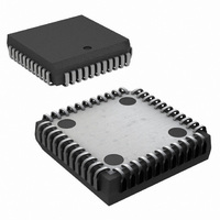
Manufacturer Part Number
NS16C2552TVAX/NOPB
Description
IC UART DUAL 16BYTE 44-PLCC
Manufacturer
National Semiconductor
Datasheet
1.NS16C2552TVAXNOPB.pdf
(44 pages)
Specifications of NS16C2552TVAX/NOPB
Features
Programmable
Number Of Channels
2, DUART
Fifo's
16 Byte
Voltage - Supply
2.97 V ~ 5.5 V
With Auto Flow Control
Yes
With Irda Encoder/decoder
Yes
With Modem Control
Yes
Mounting Type
Surface Mount
Package / Case
44-LCC (J-Lead)
Lead Free Status / RoHS Status
Lead free / RoHS Compliant
Other names
NS16C2552TVAX
Available stocks
Company
Part Number
Manufacturer
Quantity
Price
Company:

Part Number:
NS16C2552TVAX/NOPB
Manufacturer:
Texas Instruments
Quantity:
10 000


D7
D6
D5
D4
D3
D2
D1
D0
A2
A1
A0
CS
CHSL
RD
WR
RXRDY1
RXRDY2
Signal
Name
5.0 Pin Descriptions
The NS16C2552/NS16C2752 pins are classified into the fol-
lowing interface categories.
•
•
•
•
Serial channel number (1 or 2) is designated by a numerical
suffix after each pin name. If a numerical suffix (1 or 2) is not
5.1 PARALLEL BUS INTERFACE
Bus Interface
Serial I/O Interface
Clock and Reset
Power supply and Ground pins
Type
IO_Z
O
I
I
I
I
I
PLCC
Pin #
N/A
15
14
10
18
16
24
20
9
8
7
6
5
4
3
2
TQFP
Pin #
48
47
46
45
44
10
13
11
20
15
31
3
2
1
9
4
8
Data Bus:
Data bus comprises eight TRI-STATE input/output lines. The bus provides bidirectional
communications between the UART and the CPU. Data, control words, and status
information are transferred via the D
Register Addresses:
Address signals connected to these 3 inputs select a DUART register for the CPU to read
from or write to during data transfer. Table 1 shows the registers and their addresses. Note
that the state of the Divisor Latch Access Bit (DLAB), which is the most significant bit of the
Line Control Register, affects the selection of certain DUART registers. The DLAB must be
set high by the system software to access the Baud Generator Divisor Latches and the
Alternate Function Register.
Chip Select:
When CS is low, the chip is selected. This enables communication between the DUART
and the CPU. Valid chip select should stabilize according to the t
Channel Select:
CHSL directs the address and data information to the selected serial channel. (Table 1)
1 = channel 1 is selected.
0 = channel 2 is selected.
IO Read:
The register data is placed on the D0 - D7 on the falling edge of RD. The CPU can read
status information or data from the selected DUART register on the rising edge.
IO Write:
On the falling edge of WR, data is placed on the D0 - D7. On the rising edge, the data is
latched into the selected DUART register.
UART Receive-ready: The receiver DMA signaling is available through this pin which is a
seperate pin on the TQFP package, while on the PLCC package it is available through the
MF pins (19, 35). When operating in the FIFO mode, the CPU selects one of two types of
DMA transfer via FCR[3]. When operating in the 16450 Mode, only DMA mode 0 is
available. Mode 0 supports single transfer DMA (and a transfer is usually made between
CPU bus cycles). Mode 1 supports multi-transfer DMA where multiple transfers are made
continuously until the Rx FIFO is empty. Details regarding the active and inactive states of
this signal are described in Section 6.5 FIFO CONTROL REGISTER (FCR) and Section 7.9
DMA OPERATION.
5
associated with the pin name, the information applies to both
channels.
The I/O types are as follows:
Type: I
Type: O
Type: IO_Z
7
-D
Description
0
Data Bus.
Input
Output
TRI-STATE I/O
AW
parameter.
www.national.com
Related parts for NS16C2552TVAX/NOPB
Image
Part Number
Description
Manufacturer
Datasheet
Request
R

Part Number:
Description:
National Semiconductor [8-Bit D/A Converter]
Manufacturer:
National Semiconductor
Datasheet:
Part Number:
Description:
National Semiconductor [Media Coprocessor]
Manufacturer:
National Semiconductor
Datasheet:
Part Number:
Description:
Digitally Controlled Tone and Volume Circuit with Stereo Audio Power Amplifier, Microphone Preamp Stage and National 3D Sound
Manufacturer:
National Semiconductor
Datasheet:
Part Number:
Description:
Digitally Controlled Tone and Volume Circuit with Stereo Audio Power Amplifier, Microphone Preamp Stage and National 3D Sound
Manufacturer:
National Semiconductor
Datasheet:
Part Number:
Description:
AC97 Rev 2 Codec with Sample Rate Conversion and National 3D Sound
Manufacturer:
National Semiconductor
Part Number:
Description:
Manufacturer:
National Semiconductor
Datasheet:
Part Number:
Description:
Manufacturer:
National Semiconductor
Datasheet:
Part Number:
Description:
General Purpose, Low Voltage, Low Power, Rail-to-Rail Output Operational Amplifiers
Manufacturer:
National Semiconductor
Datasheet:
Part Number:
Description:
8-bit 20 MSPS flash A/D converter.
Manufacturer:
National Semiconductor
Datasheet:
Part Number:
Description:
Low Noise Quad Operational Amplifier
Manufacturer:
National Semiconductor
Datasheet:
Part Number:
Description:
Quad Differential Line Receivers
Manufacturer:
National Semiconductor
Datasheet:
Part Number:
Description:
Quad High Speed Trapezoidal? Bus Transceiver
Manufacturer:
National Semiconductor
Datasheet:
Part Number:
Description:
Dual Line Receiver
Manufacturer:
National Semiconductor
Datasheet:
Part Number:
Description:
TTL to 10k ECL Level Translator with Latch
Manufacturer:
National Semiconductor
Datasheet: